With all the hype surrounding the potential use of glass interposer substrates and hybrid bonding, I thought taking a deep dive look at the recent publication “Flip Chip on Glass Core Substrates with Microbump and Cu-Cu Hybrid Bonding” ,which appeared in the IMAPS Journal of Microelectronics and Electronic Packaging, by Advanced Packaging stalwarts John Lau , Mike Ma and co-workers at Unimicron, was warranted. It is a wonderful example of how complex advanced packaging can be and exemplifies the kind of work needed to be done if one wants to compete in this arena.

Background
Unimicron first reviews the extensive work that has been done at GaTech during the past two decades, then details the commercial announcements that have been made so far by Absolics (SK Hynix), Intel and TSMC. While IFTLE would still question the Intel announcement due to its current financial situation, the TSMC statements and Absolics factory in Georgia appear real.
During the TSMC 2025 North America Technology Symposium, the company announced its chip-on-panel-on substrate (CoPoS) to replace some of its chip-on-wafer-on-substrate (CoWoS) for high-performance computing (HPC) driven by artificial intelligence (AI). The CoPoS products are planned to be shipped in late 2028 and the glass panel size is 310mm x 310mm.
Absolics, a US subsidiary of South Korean SK Group (SKC) in Georgia announced that it will be manufacturing glass-core package substrates and the TGV-interposers in 2026.
The Unimicron authors state that “…reliability issues because of the glass-core substrate are seldom discussed, especially the semiconductor packaging interconnects such as the solder joint reliability.”
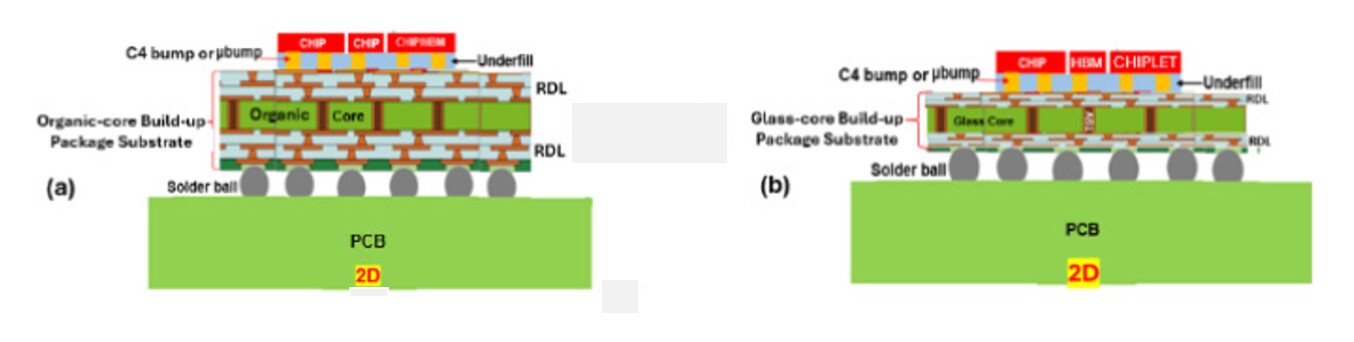
Two problems of flip chip on glass-core package substrate were investigated (Figure 1).
- The first problem deals with the flip chip on glass-core package substrate with microbumps
- The second problem deals with the flip chip on glass-core package substrate with Cu-Cu hybrid bonding.
The fabrication process of through glass vias (TGV) is very different from that of silicon vias (TSV). Most TSVs are fabricated by the deep reactive-ion etching (DRIE), however, today most of the TGVs are fabricated by laser drilling, such as the laser induced deep etching (LIDE) developed by LPKF.
The most common used glass materials are the SCHOTT AF 32 alkali-free flat glass and the CORNING HPFS 7980 high purity non crystalline fused silica glass. Both materials have low coefficient of thermal expansion (CTE), which are close to that of silicon.
The TGV are formed by high-speed laser and the modified area of the glass subsequently removed by anisotropic wet chemical etching, (HF or NaOH). This is followed by the metallization of the seed layer such as Ti/Cu, and then, electroplated Cu to fill the vias.
The process flow for fabricating the RDLs of the TGV is very similar to the RDLs of TSV as is shown below for (a) L/S ≥ 2µm and (b) for L/S < 2µm (Figure 2).
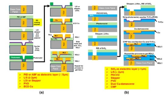
Figure 2: Fabrication process flow of TGV RDLs: (a) L/S ≥ 2µm (b) L/S < 2µm.
Flip chip on glass-core package substrate with microbumps
According to Unimicron, problem-one in these structures is due to the accumulated equivalent inelastic strain in the µbump on glass structures which is significantly higher than for equivalent organic-core substrates as shown below.


Flip chip on Glass-core Package Substrate with Cu-Cu Hybrid Bonding.
There are two build-up layers on the glass-core’s top and bottom sides which are fabricated by plasma-enhanced chemical vapor deposition (PECVD) for the SiO2 dielectric layer (1.5µm-thick) and Cu dual-damascene for the metal layer (1.5µm-thick). The Cu-pad pitch is 10µm. The glass-core substrate is flat enough to perform Cu-Cu hybrid bonding.
Warpage
The deformation of the flip chip bonded on the glass-core package substrate with Cu-Cu hybrid bonding are larger than the structure with µbumps. The deformation of this size of chip is acceptable in most applications.
For flip chip solder interconnects, the focus is on the inelastic strain while for flip chip Cu-Cu interconnects, the focus is on the stress. The strains in Cu-Cu bonding are very small.
The accumulated equivalent (von Mises) stress at the corner Cu-pads is located at the interface between the Si chip and the Cu-pad. This is due to the large thermal expansion mismatch between the silicon and Cu.
The accumulated equivalent inelastic strain contours at the corner solder balls occurs near the interface between the solder ball and the PCB. This is due to the large thermal expansion mismatch between the glass-core and the PCB.
Unimicron summary
- Organic-core build-up package substrate is here to stay and used at huge volume for a long time. Glass-core build-up package substrate can seamlessly integrate optical interconnects and will initially be used for niche applications.
For flip chip bonded to glass-core and organic-core substrates with µbumps.
- For the µbump solder joint, the maximum accumulated equivalent inelastic strain is smaller in the structure with glass-core substrate than with organic-core substrate.
- For the C4 solder joint, the maximum accumulated equivalent inelastic strain is more than two times larger in the structure with glass-core substrate than with organic-core substrate.
- It is recommended that the CTE of the glass-core substrate should be closer to the CTE of the PCB (not to the CTE of Si chip) because there is no underfill protection of the C4 or BGA solder joints on the PCB, especially for larger glass-core substrates.
For flip chip bonded to glass-core substrate with Cu-Cu hybrid bonding.
- Unlike organic-core substrates, the glass-core substrates are flat enough to perform Cu-Cu hybrid bonding.
- For extremely fine-pitch, high-density, and high-performance applications, the L/S of the RDLs of the glass-core substrate are usually less than 2µm. The dielectric layer (SiO2) can be fabricated by PECVD and the metal layer by dual-damascene Cu + CMP (chemical-mechanical polishing).
- The warpage of the flip chip bonded on glass-core substrate with Cu-Cu hybrid bonding are very similar to that of the flip chip bonded on glass-core substrate with µbumps, except the magnitudes. The magnitudes of the Cu-Cu hybrid bonding are larger than those of the µbumps. This is because of the relaxation of the µbumps.
- The maximum accumulated equivalent inelastic strains in Cu-Cu hybrid bonding are very small.
- The maximum accumulated equivalent (von Mises) stress occurs at the interface between the Si chip and the Cu-pad.
- The maximum accumulated equivalent inelastic strain occurs near at the interface between the solder ball and the PCB.
- The accumulated equivalent inelastic strain per cycle is 16.02%, which is smaller than that with µbump (19%). However, it is still quite high for the solder joint reliability. A larger CTE for the glass-core substrate is recommended. By increasing the CTE of glass core the warpage of the structure is reduced.
For all the latest in Advanced Packaging stay linked to IFTLE…………………………….


