At the recent IMAPS Onshoring Workshop, Greg Kleese, Director of Aero & Defense Business Development, GlobalFoundries, made the presentation “GlobalFoundries Advanced Packaging and Photonics Center”. Since the slides were labeled “Approved for public release, distribution unlimited” I can give you a taste of what he had to say.
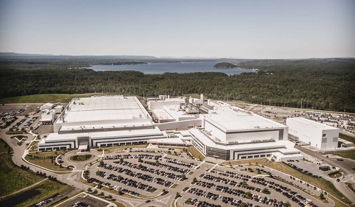
GlobalFoundries’ New York Advanced Packaging and Photonics Center (NYAPPC), is supported by funding from New York State and the U.S. CHIPS Act.
Customer solutions supported in this facility reportedly include:
- Silicon Photonics advanced packaging, assembly, and testing of customer products on GF’s optical and electrical 45CLO platform. This includes delivery of complete optical modules for Co-Packaged Optics (CPO) for AI Data Centers
- Production capabilities for advanced packaging, wafer-to-wafer bonding, assembly, and testing of 3D and heterogenous integration (HI) for our most advanced technology platforms such as 12LP+ and 22FDX.
- Advanced packaging, bump, assembly, and testing for aerospace and defense customers under its Trusted Foundry accreditation (Figure 1).

GF offers all of the following advanced packaging architectures:
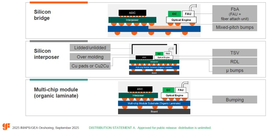
As IFTLE has discussed previously, GlobalFoundries is one of the few onshore sites to offer qualified Si interposer technology.

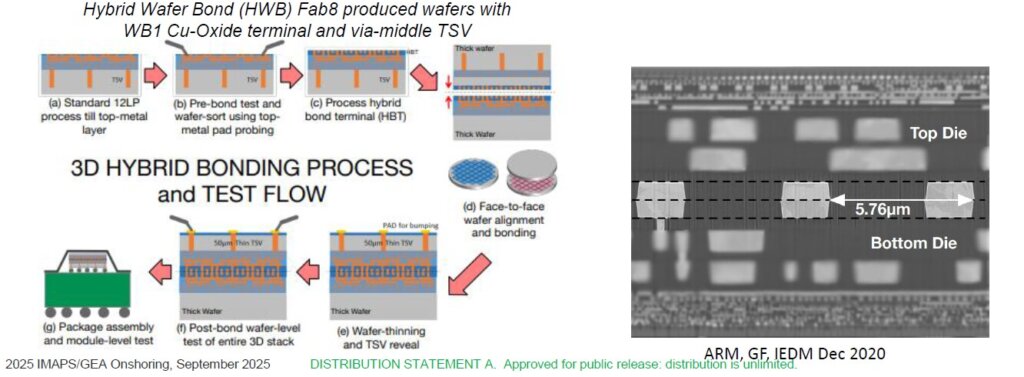
They are also one the few on shore sources of hybrid bonding technology stating that their “SLATE” hybrid bonding platform is “…volume-production ready.”
For all the latest on Advanced Packaging stay linked to IFTLE……………………………..


