
Australian semiconductor technology company Syenta has raised A$8.8 million in Pre-Series A funding to commercialize a breakthrough in chip packaging that could unlock the next generation of AI and high-performance computing. The round was led by Investible, with participation from Blackbird Ventures, In-Q-Tel, SGInnovate, OIF Ventures, Salus Ventures, Jelix Ventures, Wollemi Capital Group, and Brindabella Capital.
Spun out of the Australian National University, Syenta has developed a transformative approach to semiconductor manufacturing with its proprietary Localized Electrochemical Manufacturing (LEM) technology. This novel approach enables micron-scale resolution in advanced semiconductor packaging, offering a scalable solution to the pressing memory bandwidth bottlenecks in AI computing.
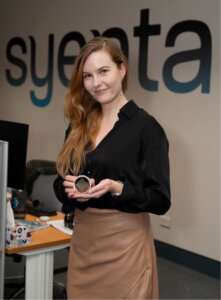
“LEM is the foundation for a new generation of chip packaging,” said Dr Jekaterina Viktorova, CEO and Co-Founder of Syenta. “It offers the scale, performance and manufacturability needed to overcome the critical ‘memory wall’ throttling AI systems today.”
As AI models continue to grow in size and complexity, they need to move more data between memory and processors. But the speed or “memory bandwidth” at which data can move hasn’t kept up with how fast processors have become. This growing mismatch is known as the “memory wall,” and it’s now one of the biggest bottlenecks in AI performance. In the last 20 years, processor speeds have improved about 60,000 times, but memory bandwidth has only improved 100 times, and the connections (called interconnects) between components have only improved 30 times.
This is where Syenta’s technology comes in. LEM is a new way of building the physical connections inside chips, enabling manufacturers to create much denser and more precise wiring, so memory and processors can sit closer together and exchange data much faster and more efficiently.
What makes LEM different is that it doesn’t use the traditional, expensive methods (like photolithography), which are too slow and complex for today’s needs. Instead, it uses a simpler, more scalable process that:
- Accelerates path-to-market by reducing cycle time and design-to-production time
- Uses 12 manufacturing steps instead of 23 used in the current semi-additive process
- Reduces total cost of ownership by 70%
- Achieves panel-level scalability for higher throughput at a lower cost
- Cuts down on waste and emissions
This positions Syenta’s technology as a key enabler of new chip designs (like 2.5D and 3D stacking), which are essential for the next generation of AI hardware, edge computing, and datacentre infrastructure – where speed, efficiency, and power usage matter most.

Originally developed in Australia, Syenta’s technical credibility was recognized on a global scale in 2024 when it was selected for ASTRA, the flagship accelerator by Applied Materials. The selection followed a successful feasibility project with Applied Materials, the world’s largest semiconductor equipment manufacturer.
“Being selected for ASTRA is a major milestone for Syenta – it puts us shoulder-to-shoulder with the industry’s most disruptive innovators and gives us direct access to leaders in the electroplating world, global foundries, OSATs and materials giants,” said Dr Viktorova. “It validates LEM as a serious platform for global semiconductor manufacturing.”
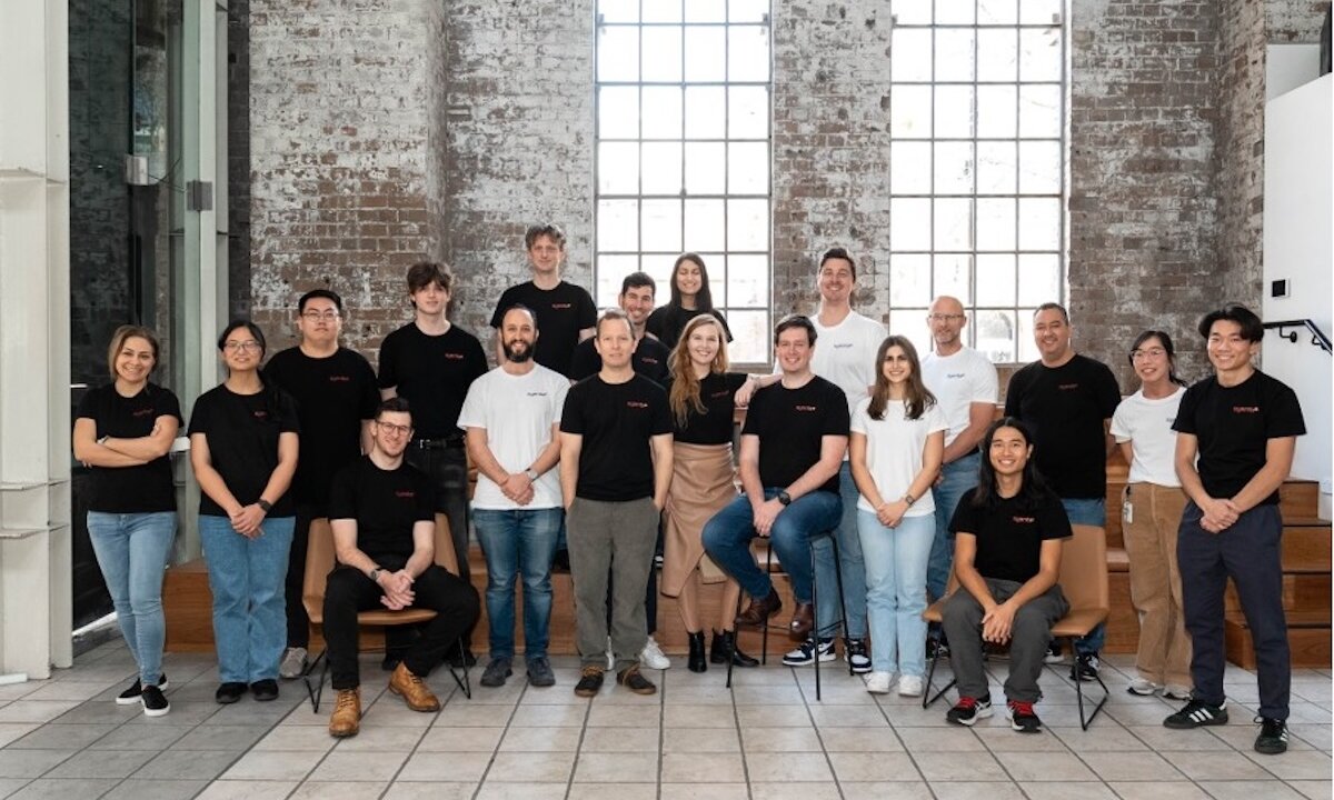
Syenta is now seeing significant traction with its LEM process, and is engaged with early access partners across the semiconductor supply chain. The company’s leadership team combines deep scientific expertise with executional strength: Dr. Viktorova, a printed electronics chemist; Professor Luke Connal, a global expert in materials science; CTO Ben Wilkinson, with a background in photovoltaics and applied physics; and COO, Zach Dowse, a neuroscientist and experienced operator.
“Syenta is a key technology enabler for the next generation of AI infrastructure and high-performance computing (HPC) chips, particularly as semiconductor chip fabrication levels are unable to keep up with current demand for generative AI infrastructure”, said Nicholas Ooi, Lead Investor at Investible. “The team’s deep academic and materials development experience, together with their patented LEM technology, positions Syenta to become a world-leader in semiconductor advanced packaging.”


