
SUNNYVALE, Calif., Mar 20, 2024 – Advanced Semiconductor Engineering, Inc. (ASE), a member of ASE Technology Holding Co., Ltd. (NYSE: ASX, TAIEX: 3711), today announced that it has extended its advanced interconnect technology under the VIPack™ platform to meet the accelerating demand for complex chiplet integration for artificial intelligence (AI) applications. This interconnect extension advances roadmap capabilities from a chip-on-wafer interconnect pitch of 40um to 20um through advanced micro bump technology. Such new interconnect solutions are crucial for architects seeking to accomplish creativity and scale across 2D, or side-by-side, solutions as well as newer vertically integrated solutions, such as 2.5D and 3D packaging capabilities, under ASE’s VIPack™ platform.
As the chiplet design approach accelerates, ASE’s advanced interconnect technology allows designers to consider innovative, high-density chiplet integration options where there might normally be chip IO density limitations for true 3D layered IP block considerations. ASE’s micro bump technology allows for a reduction in pitch from 40um down to 20um using a new metallurgical stack. While advances in micro bump have extended the existing capabilities of silicon-to-silicon interconnect, this technology has helped to facilitate other development activities that allow even further pitch reductions.
When considering chiplets or IP block disaggregation of an SoC, there may be a high number of connections to interface with other areas of the design. This drives a higher number of connections that may be space limited due to the small size of the IP block. Fine pitch interconnect capabilities enable a 3D integration capability as well as a higher density for high IO memory considerations.
With the global AI market expected to grow exponentially throughout this decade, ASE is delivering advanced interconnect innovations that meet complex chip design and system architecture requirements to lower overall manufacturing costs and enable faster time to market. The extended chip level interconnect technology opens up more applications for chiplet consideration, targeting not just high-end applications such as AI, but also other key products such as mobile AP, microcontrollers, and more.
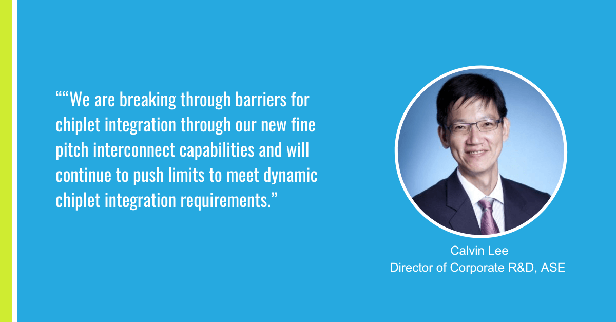
“Silicon-to-Silicon interconnect has moved from solder bump to micro bump, and as we move into the AI era, there’s a growing need for further interconnect technology advancements that deliver enhanced reliability and optimized performance across a broad spectrum of nodes – and this is where ASE has stepped up,” commented Calvin Lee, Director of Corporate R&D, ASE. “We are breaking through barriers for chiplet integration through our new fine pitch interconnect capabilities and will continue to push limits to meet dynamic chiplet integration requirements.”
“Our customers require transformative technologies that enable their product roadmaps, and advanced interconnect technologies such as micro bump, in combination with the VIPack structures, help to address performance, power, and latency challenges,” added Mark Gerber, ASE’s Senior Director of Engineering & Technical Marketing. “ASE’s advanced interconnect technologies present compelling options for customers that seek increasingly finer pitch solutions for overall performance improvement, scalability achievement, and power advantage.”

“We are pleased that ASE’s VIPack™ momentum continues through creative interconnect innovations that overcome limitations and align with dynamic application requirements,” added Yin Chang, Senior Vice President of Sales & Marketing at ASE. “At ASE, we empower our customers to explore and discover new performance and sustainable efficiencies in every single semiconductor design and system solution.”
ASE’s VIPack™ is a scalable platform that is expanding in alignment with industry roadmaps, supported by its Integrated Design Ecosystem™ (IDE), a collaborative design toolset optimized to systematically boost advanced package architecture.


