
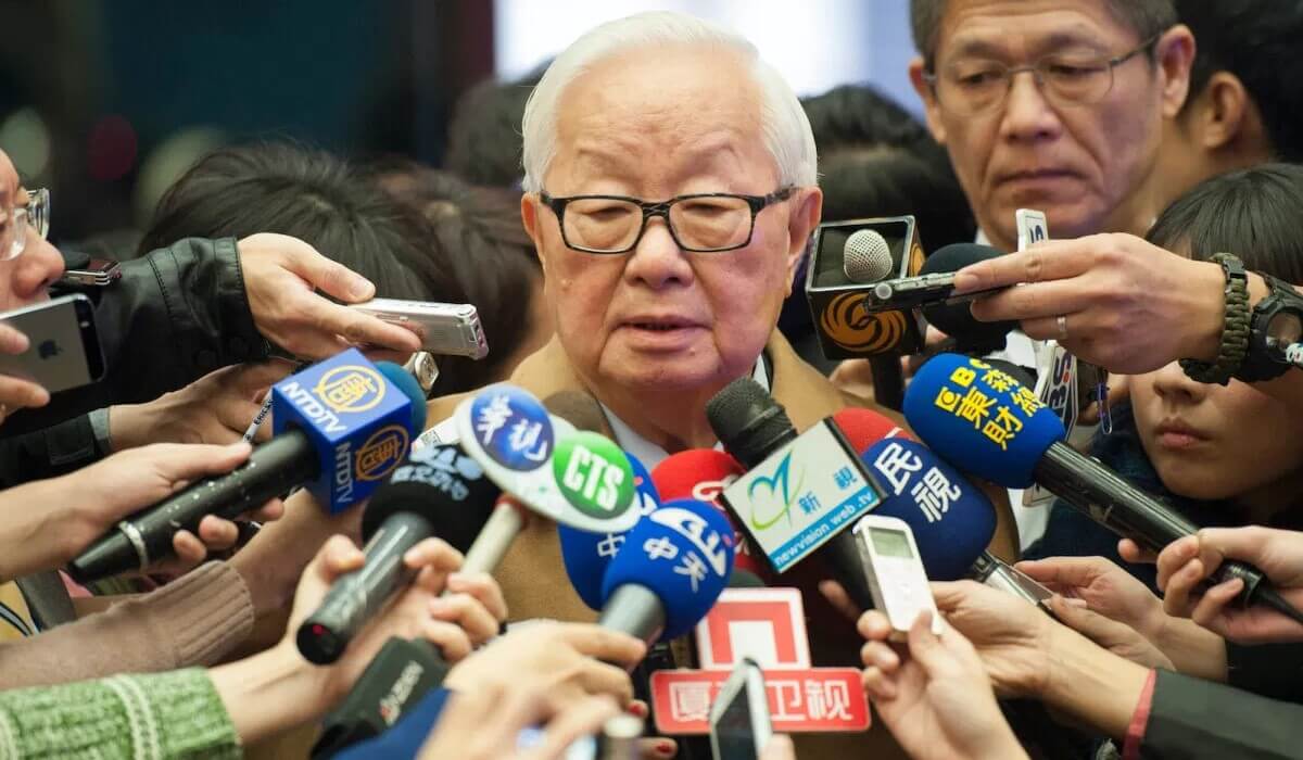
Morris Chang, retired long-time CEO of TSMC, was recently quoted in the Taipai Times as saying “US efforts to increase onshore manufacturing of semiconductors is wasteful and an expensive exercise in futility due to a lack of manufacturing talent and high costs”. Chang made the remarks in an interview with the Brookings Institute. Chang called the US government’s efforts to increase onshore chip manufacturing by spending tens of billions of dollars, “..a very expensive exercise in futility.”
He continued “…the US used to have strong talent as Taiwan does now …. however, after the 1970s, young talent in the US migrated to high-paying professions such as finance or consulting, rather than working for technology companies such as GE or IBM.” (IFTLE says OUCH the truth hurts.)
Chang contends that another challenge is high manufacturing costs. He points to their fab in Oregon, which was established in 1997, where the chips made at the Oregon factory cost 50 percent more than those made by TSMC’s factories in Taiwan.
Regarding TSMC’s new $12B gigafab in Arizona, which aims to manufacture 5-nanometer chips by 2024, Chang said that current chairman Mark Liu made the decision at the insistence of the US government.
Chang concluded that “The US will increase onshore manufacturing of semiconductors somewhat…… at a very high-cost increase, high unit costs, but non-competitive in the world market when competing with factories like TSMC.”
Regarding Intel CEO Gelsinger’s remarks that “Taiwan is not safe,” Chang said he assumes that there will not be a war. “If there is no war, then I think US efforts to increase onshore manufacturing of semiconductors is a wasteful and expensive exercise in futility” and “If there is a war, we all have a lot more than just chips to worry about!”
Huawei Turns To Packaging to Circumvent US Sanctions
According to reports at Toms Hardware, Huawei has patented a chip stacking process that could theoretically help it avoid US sanctions.
There is still a question as to whether Huawei can actually take advantage of its innovation, given that foundries cannot produce chips for the company without an export license from the U.S. government, but Huawei believes that it can.
Huawei and its chip design subsidiary HiSilicon are blacklisted by the US Government, and this requires all companies making silicon for them to apply for an export license since all semiconductor production involves technologies developed in the U.S., Huawei can’t access any modern node (e.g., TSMC’s N5), and therefore has to rely on mature process technologies.
Huawei indicated that since modern leading-edge process technologies are progressing relatively slowly, multi-chiplet designs in 2.5D or 3D packages are a way for chip designers to keep meeting the expectations of new features and performance. Innovative chip packaging and chiplet interconnection technologies as well as 3D stacking are ways for the company to get the performance it needs to be competitive with older nodes.
As recently reported by Digitimes, Huawei aims to use its hybrid 3D stacking method for its upcoming products. There remains a question as to whether the method requires any tools or technologies that the U.S. government may deem cutting-edge and not grant an export license (after all, most of the fab tools use technologies that originated in the USA).

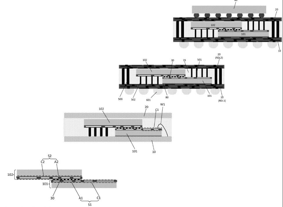
Through silicon vias (TSVs) add complications and costs to the packaging process, so Huawei decided to invent an alternative solution without TSVs. What Huawei designed is a technology where two chips / chiplets overlap each other inside the package, saving space, but don’t sit directly on top of each other like classic 3D packages.
Huawei’s method uses overlapping parts of the chiplets to establish the interconnection. The chiplets still have their own power delivery pins connected to their own redistribution layer (RDL) using a variety of methods.
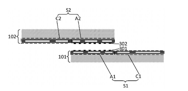
Huawei’s process involves flipping one of the chiplets upside down before connecting to another (or others). It also requires building at least two redistribution layers to deliver power (e.g., two chiplets means two RDLs), which is not low-cost since it adds several additional process steps. The RDL of one of the chips can be used to connect things like memory, thus saving space.
It is difficult to stack hot logic dies on top of each other, due to cooling issues. Huawei’s method increases the surface size of the stack, which reportedly simplifies cooling. The stack is smaller than a 2.5D package, which is important for mobile applications like smartphones, notebooks, or tablets.
SMIC, with whom Huawei reportedly plans to build a fab, is also betting on advanced packaging and interconnection technologies as a way to get around sanctions imposed by the U.S. government. The company cannot get access to manufacturing tools required to make chips using sub-10nm fabrication technologies, so advanced packaging and interconnection methods are crucial for SMIC as well.
For all the latest in Advanced packaging stay linked to IFTLE…………………..


