

Over the years on 3D inCites, we’ve discussed the debate about the advantages and disadvantages of using glass substrates for advanced packaging applications. Thanks to ongoing research and development, a clear path has emerged for the use of glass in two key areas: as carrier substrates for high-density fan-out (FO) packages and as glass interposers for 2.5D integration. At ECTC 2019, I spoke with two companies who have are succeeding in bringing these technologies to market, respectively: Corning Glass and Samtec Microelectronics.
Glass Carriers for Fan-out
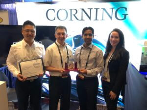
Corning won the 2019 3D InCites’ Award for Materials Supplier of the Year for its glass Advanced Packaging Carrier (APC), which was developed especially to address in-process warp issues for high-density FO packaging. This is the first time a glass manufacturer has received the award. Wanting to know what made these carriers different from the company’s standard carriers used in low-density FO, I spoke with Joseph Canale, Sr. applications engineer, and Jason Lee, account manager for Korea.
Canale explained that in-process warp is an ongoing challenge for advanced FO packaging that must be addressed to achieve high yields, particularly as FO penetration in mobile electronic products continue to drive toward thinner packages with enhanced functionality.
During FO processes, Si dies, molding compound materials, and redistributions layers (RDLs) are built up on the carrier to form a composite structure. The amount of warpage to the final wafer is influenced by three elements:
- Coefficient of thermal expansion (CTE) mismatch between all the materials involved
- The Young’s Modulus (YM) of the glass carrier
- The thickness of the glass
The key, then, for designing carriers that are successful in minimizing warp is to decrease CTE mismatch while increasing both YM and glass thickness. Glass provides the ideal material for this, explained Canale, because all these knobs can be tuned to customer specifications. In comparison with standard glass carriers, Corning’s APC product line offers higher granularity options ranging from 4.9-12.6 to adjust its CTE matching and 20% higher YM so it can be made as thin as possible while retaining high stiffness.
In development for two years, the APCs were introduced to the market in January, explained Lee. He said these are not off-the-shelf solutions. “We work closely with our customers to target real-world challenges and find the right combination that works for them by testing small batches,” he explained. “As the technology matures, we will be able to build a portfolio of choices and selections for high volume manufacturing.”
While Corning is also developing glass interposers with through glass vias (TGV) for 3D ICs, the company has been focusing on APCs because Yole Développement’s market research has determined that for consumer products, 3D IC with through silicon vias (TSVs) or TGVs are still too expensive for consumer devices. Advanced FO is more affordable and provides advantages such as the elimination of a substrate, finer lines, and improved thermal and electrical performance over incumbent technologies. It made strategic business sense to focus efforts on APCs. However, both wafer and panel level TGV is also on Corning’s roadmap.
Glass Interposers for High-Performance Microelectronics
While it is true that glass interposers with TGVs have not reached consumer applications, Steve Groothuis, CTO, Samtec Microelectronics, says there are several emerging vertical markets for which they are ideal. These include military and aerospace, biomedical, and telecommunications. Samtec has focused efforts on developing Glass Core Technology specifically to meet the needs of these markets.
Groothuis explained that these core technologies often utilize borosilicate glass, fused silica, and other glass-ceramic materials. Samtec’s unique combination of different metallization methods combined with deep silicon expertise, enables customers to experience ultimate flexibility.

Samtec is navigating a distinct path forward with its Glass Core Technology as Moore’s Law slows. Various 2.5D and 3D packaging methods (e.g., die and substrate stacking) are evolving using glass interposers and substrates, which continue to enable smaller, denser, and faster applications.
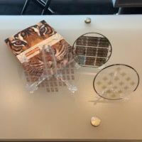
Currently, Samtec offers a process for metallization of TGVs, combined with RDL patterning on glass for low-loss fan-out chip to package interconnects (Figure 3). Groothuis said this metalized glass interposer is ready for flip-chip applications with either solder bumps or copper pillars. These are targeted mainly to high-performance RF applications for telecommunications and mil/aero markets.
In the biomedical space, the company will develop glass solutions for lab-on-a-chip applications by creating microfluidic channels and shaped vias in glass or fused silica substrates that are ideal for microfluidics along with electrical and possibly optical interconnects.
A Serious Contender
Glass as an alternative to silicon for both interposers and glass carriers has certainly come along way over the past few years. I expect further development will make it a serious contender and an enabler of heterogeneous integration in years to come. ~ FvT


