
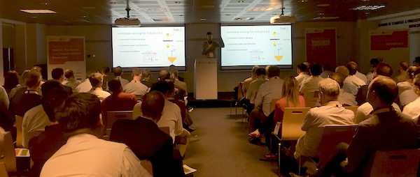
The technology showcases at the European MEMS and Sensors and Imaging Sensors Summits give start-ups and established companies alike ten minutes to pitch their latest innovation to the crowd, after which attendees vote for the best. The competition is fierce, and the prize – a free booth the following year – is much sought after. Each summit has one winner, and they were announced during the gala dinner.
MEMS and Sensors
On the MEMS side, entries ranged from tools to design and build MEMS and MEMS-based technologies used to manufacture other devices, as well as sensors themselves, including:
- A cloud-based simulation tool for MEMS designers that was demonstrated for piezoelectric micromachined ultrasonic transducers (PMUT) fingerprint sensor arrays.
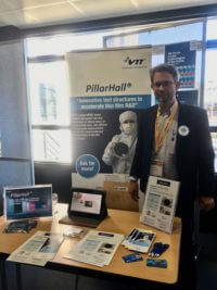
- A MEMS-based, all-silicon test structure used to non-destructively measure ALD film thickness for conformality, even on difficult 3D structures.
- A MEMS die-attach adhesive designed for optimum stress decoupling. It can also be used as an ASIC coating, capable of shielding five faces of the die from IR radiation.
- A handheld spectrometer that uses quantum cascade lasers (QCL) and photoacoustic detection for multi-gas sensing, targeted towards addressing the pollution problem.
- A high-performance, low-power MEMS accelerometer with advanced features that make it ideal for a variety of wearable and IoT applications. Here, it was demonstrated for use as a step counter, and also in a smart home application for detecting open windows.
The diversity of these technologies made it really tough to pick the best, as it wasn’t an apples-to-apples comparison.
My money was on the die-attach material from Delo, probably because of my interest in technology that enables heterogeneous integration and packaging. Plus, the stuff is pretty cool – and it’s such an elegant solution for critical issues. No bells and whistles – just a unique chemistry that gives it a low Young’s Modulus, high shear strength, a large aspect ratio, and speedy dispense.
The rest of the crowd had other ideas, however. The MultiSense handheld spectrometer won for its ability to detect up to 10 gasses, as well as complex molecules like hydrocarbides and blood constituents. Enabled by QCL and MEMS-microphone based acoustic detection, the device has no moving parts, is compact, low power, and low cost. And it appeals to the “make the world a better place” mindset.
Imaging and Sensors
On the imaging side, the entries brought emphasis to the fact that most imaging innovation is in technologies that enable machine vision applications, rather than technologies that improve photography. They included:

- A single photodiode for 3D imaging based on time-of-flight. This technology was integrated into an ASIC for a wearable device for vital signs monitoring.
- A passive infrared detection array that transforms body heat into electronic signals. These PyrOnic sensors are integrated with dedicate CMOS and a new optical system to create a low-cost, imaging system for applications like human detection or posture and gesture recognition for smart buildings, assisted living, and more.
- A single imager 3D lidar and 2D camera for autonomous vehicles. This solid-state lidar outputs 3D cloud points and 2D images for long-range detection and tracking of obstacles and road users.
- An image compression technology that uses quantum physics techniques to compress raw image data at a 10-1 ratio, removing artifacts while preserving image data.
- An ASIC design methodology using mmWave technology for imaging applications by leveraging the property of the wave to detect objects. Systems can be implemented in silicon (CMOS, SiGe, SOI) at a lower cost than current GaAs approaches.
While I was rooting for DotPhoton, the image compression technology, because I tried out the app myself, and could see the benefits for improved image quality for machine vision applications. For example, in automotive applications, this image compression algorithm removes artifacts from image data so that the car can distinguish between a baby carriage and a grocery cart.
However, the award went to another automotive imaging application that addressed similar challenges. Xenomatix 3D solid-state lidar products measure an analyzes a car’s surroundings, providing more than just 2D images. The company claims it provides a “360° precise and high-resolution sensing under all light and weather conditions and at any driving speed.”
Be sure to stop by the winner’s booths at next year’s MEMS and Imaging Summits, which will take place September 25-27 2019, in Grenoble, France. In the meantime, you can catch the MEMS and Sensors Executive Congress Technology Showcase in Napa, October 28-30.


