

Finally! After a year’s worth of guesswork, Samsung’s 3D V-NAND Flash cell has been revealed.

Thanks to the expertise of Chipworks we can see how the memory array looks in the 86 Gbit 32-layer 2nd generation V-NAND. Figure 1 shows Chipworks’ beautiful cross section. My intention here is to explain the structure, compare it with what I have written about before and, of course, give my opinion.
Previously, I had guessed at the cell size and structure based on Samsung’s ISSCC February 2014 presentation about their 128 Gbit 24-layer 1st generation V-NAND. Then, Samsung introduced their SSD 850 Pro containing their 86 Gbit 32-layer 2nd generation V-NAND. It took detective work by others to allow me to guess at their cell size and structure.
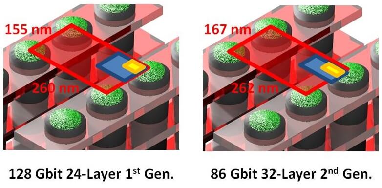
Figure 2, taken from my previous article, shows the derived cell sizes and structures from information thus cobbled together.
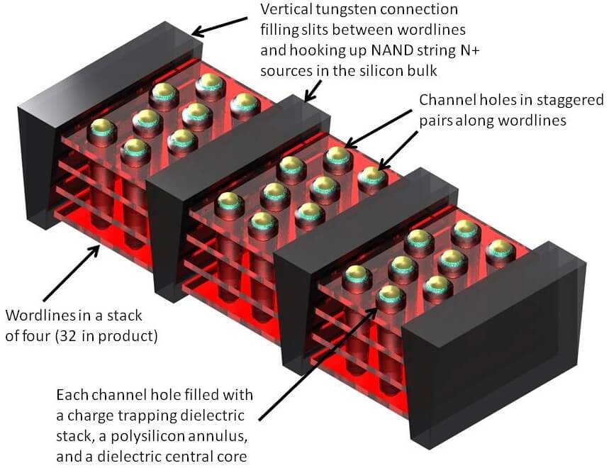
Well, now we have the real cell structure thanks to Chipworks. How does it compare with the guesswork? Figure 3 shows a generic vertical channel 3D NAND based on Chipworks’ cross section. The wordlines are shown in the same direction as in Figure 2 for ease of comparison (in other words, sweeping from bottom left to top right).
If you need a reminder on how such a vertical channel 3D NAND works, have a quick glance at my first series of blog posts.
On first inspection, Samsung’s product version V-NAND in figures 1 and 3 looks different from what is sketched out in figure 2. But let’s look more closely.
The three main architectural differences are:
- Wider wordlines encompassing pairs of channel holes instead of narrow wordlines with single lines of channel holes.
- Staggered pairs of channel holes placed along length of wordlines.
- Slits between wordlines filled with a conductor instead of a dielectric.
Remember though, that there is still risk in assuming that Figure 3 is totally accurate based on Figure 1. The probability of accuracy is high, but best to wait for the more detailed analysis from Chipworks to make sure. Nevertheless, assuming Figure 3 is accurate, why would Samsung make such changes from what they have published in the academic literature that was used to generate figure 2?
First of all, changes from device-based academic papers to what eventually appears in a product are not strange since product-level optimization usually demands this. My guesses for these changes are the following:

- Wider wordlines allow lower resistance in each wordline which may be important for read and program speeds. Such a wide wordline also allows placing more channels side by side (two in this case) in a line between slits. Doing this means that the relatively wide slit size is divided among more cells and has less of an impact on cell size compared to the case shown in Figure 2. The encouragement to do this may have been overwhelming given the wide-looking slit in Figure 1 (now filled with tungsten).
- Staggering the pairs of channel holes allows a slight reduction in cell size in the direction of the wordline and so counteracts other effects that may increase cell size such as wider slits that need to be filled with conducting material.
- Slits filled with conductor, probably tungsten, allow metal strapping and therefore lower resistance of the N+ doped NAND string sources in the bulk of the silicon. Again, this may have been absolutely necessary to avoid voltage drops along otherwise high resistance source lines during read, program and erase. Figure 1 may actually show the metal filled slits punching through the N+ doped sources and connecting to a p-doped well underneath although we can’t be certain. If it does, it would short the sources to their wells which has been done before by Samsung in their more conventional thin-film transistor version of their TANOS NAND about eight years ago.
In summary, Samsung’s product 86 Gbit 32-layer 2nd generation V-NAND looks similar to what has been guessed at but with interesting adjustments. The question though is what is the cell size since this is the major factor for cost per bit? Figure 4 shows a red rectangle marking out the area of two cells. The cell size would be half this area. Note that the slit width is therefore divided by two as its contribution to cell area.

Since Chipworks did not provide dimensions in their cross section, it is difficult to know what the cell pitches are in Figure 4. However, what can be said with some certainty is that the effective cell area will be about 150nm by 260nm since these numbers “fit in” with the “top down” calculations based on die size, array efficiencies, numbers of layers and capacities as given in figure 2.
It appears therefore that the product level optimizations that Samsung have had to go through in their 86 Gbit 32-layer 2nd generation V-NAND have not resulted in a smaller cell than their ~ 25F2 number where F is held at 40nm.
Let me say first of all, hearty congratulations to Samsung on an amazing engineering feat in making a real product out of their vertical channel V-NAND technology.
Now that that is out of the way, we need to consider the following. We have had to wait almost exactly a year from Samsung’s Flash Memory Summit 2013 announcement of V-NAND in mass production to actually (almost) figuring out cell size and structure. This contrasts with the usual approach where stand-alone Flash cell size in a new technology is displayed with pride by its inventor at any one of the major technical conferences.
In addition, the market chosen by Samsung (least cost sensitive) tells me that the original motivation of lowering bit cost presented in their original technical paper in 2009 (where this approach was called “TCAT”) seems to have faded away from view.
So, do I descry the “Spires of El Dorado”? Yes, but they are shorter than we initially thought and, to me at least, look like gold plate rather than solid gold. ~ AJW


I was wondering how exactly is the 25F2 calculated?
Hi Peter,
Sorry for the delay! The 25F2 is calculated with F at 40nm (where Samsung have said that they will remain for their 3D V-NAND). 25F2 (25 times the square of 40nm) then gives about 40000 nm2 which is where the single cell per layer area is at.
Hopes this helps.
Regards
Andy
Hi Andy, it is interesting and exicting to read your blogs about SCS V-NAND. Here little infos FYI, as I know for SCS Xian fab, there are four products in productions, GV (field size: 22.5×23.8, Die:2×2, die size: 133.8mm2), and GV should be their 1st generation 24 layers product, right now, almost stop in production. CF(field size: 25.1X27.2, Die:2×4, die size:85.3mm2), CB (field size: 24.5×32.1, Die:2×4, die size: 98.2mm2) and CN(field size: 25.3×32.6, Die:4X3, 68.87mm2), and currently, the CN is in main production, and looks the trend, they are shirking the die size, probably for better yield. I am not clear which one should be the chips for 850Pro, and what the process structure difference for CF, CB and CN, could you be aboe to figure out by these info? BTW, could you be able to share a copy of the chipworks report about 850Pro chips?
Hi Ricky – Thanks for your comment. It is interesting to see how Samsung is aggressively pursuing their version of 3D NAND. It looks like the 85.3mm2 die is what Chipworks found in the 850 Pro. I think the progression of smaller and smaller die sizes is probably Samsung’s attempt at both lengthening the NAND strings vertically and improving the array efficiencies.
I don’t have the full Chipworks report but I am sure they have it for sale on their website.
Regards
Andy
Hi Andy, thanks for the comment, so based on the chipworks report, CB (field size: 25.1X27.2, Die:2×4, die size:85.3mm2) should be the chips for 850Pro, so what you think the difference between CB and CF(field size: 24.5×32.1, Die:2×4, die size: 98.2mm2)? since they have same die #/ field, the only difference is field size, In my opinion, from CB to CF, they may just want to maxmize the field area for the process efficiency, since for the scanner, the max field size could be (26mmX33mm), do you think so?
And for the CN (12 dies/field), based on your comment that smaller die sizes is probably Samsung’s attempt at both lengthening the NAND strings vertically, so how to understand it? in my understanding, lengthening the NAND strings could be only achieved by increase the layers, like from 24 to 32, or from 32 to 48.
Hi Ricky – I think your guess is as good as mine. Now that Samsung have introduced their V-NAND, total cost will be key. Therefore, they will be doing everything in their power to reduce it.
Best regards
Andy
Hi Andy, thanks for the reply. in early of this month, Samsung just announced that they started the mass production of 3bits/32 layers V-NAND chips, and the production shoubd be in Xian Fab (Since Xian Fab only for their V-NAND flash chips production). So do you think the CN type product could be their 3bits/32layers products? Thanks.
Hi Ricky, then, do you think they have decided to mass produce with CF which has larger Field Size for their production efficiency even take the loss of Net Die nearly 2 digits as the die size increases 85.3 mm2 to 98.2 mm2 ?? Is it worth to give up the net die count for the larger field size??
Hi Ricky,
It could well be and if so, Samsung has been able to shrink the die and get to 3 bits per cell compared to what was analyzed in their first 850 Pro’s.
Best Regards
Andy
Hi Andy, by SCS previous announcement that they would keep 40nm node for all their V-NAND generation, however, I read the news that for SCS latest V-NAND product-3bits/32layers, they already used 32nm node technology on it, and even they will use 24nm node technology when they go to 36layers.
Hi Ricky – That’s interesting. Please point me to the Samsung announcement where they state this.
Regards
Andy
http://www.semi.org.cn/news/news_show.aspx?ID=39468&classid=117, however, it is from one famous china website about semiconductor industry.
Thanks Ricky. I had Google translate it so I think I understand. It makes reference to a Samsung announcement on Oct 9th. Do you know where this was announced?
Regards
Andy
Hi Andy, sorry, I also tried to find the original news, however, did not get it.