

It was a much-talked-about topic this year at SEMICON West 2014 (SW2014) – this trend of semiconductor equipment manufacturer consolidation. Just in the past year, we’ve read the headlines about Applied Materials (AMAT) and Tokyo Electron ‘s (TEL) impending merger; LTX Credence’s acquisition of Multitest, Everett Charles, Technologies and atg Luther & Maelzer businesses from Dover; and most recently, the announcement of Orbotech’s acquisition of SPTS Technologies. There were others, but I highlight these because they all used SW2014 as the arena in which to make significant announcements as they reach milestones in the consolidation process.
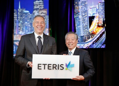
Probably the biggest buzz at SW2014 was around the unveiling of the new brand for the combined entities of Applied Materials and Tokyo Electron once the merger is complete. The new name is – Eteris (say “eh-TAIR-is.”) which, according to a blog post on the AMAT website “is derived from the concept of ‘Eternal Innovation for Society,’ to capture our commitment to creating and enabling technology innovations that improve the way people live.” The blog also describes the logo, saying it “celebrates our role in realizing the incredible possibility of technology. At the heart of the mark, the bright green anchor symbolizes the energy of our company, the power of our technology and the foundation of innovation we provide to enable customer success. From there, its bright colors and new dimensions expand, representing the many innovations that Eteris will make possible every day around the world.”
It was interesting to hear all the side-chatter about the new name. The most common reaction was surprise that two major companies with such solidly established brands didn’t picked one or the other, but set out on the arduous and risky journey of building an entirely new brand. But after catching snippets of such talk at networking functions and on the show floor, it hit me that there was no better venue to make this announcement and let the powers of networking do its job. While the companies will likely have to correct pronunciation of the name for some time, there’s no question that Eteris is already synonymous with the former TEL and AMAT.
The company formed by the mergers of LTX – Credence/Multitest/Everett Charles Technologies/ atg Luther & Maelzer also chose to unveil its new name shortly before SEMICON West. I chatted with company CTO, Reinhart Richter, about the motivation to change the brand, and he explained that a new brand helps consolidate the company better. The new company is named Xcerra Corporation, and comprises 5 product groups: testers, handlers, interface products, loadboards, and probe cards. LTX-Credence added test to the company, which previously offered the other four product groups.
The synergies of this particular consolidation are apparent. Richter said that until now they (Multitest/ECT/atg Luther & Maelzer) never had access to a suitable tester that could support the capability of the handler; LTX-Credence platform has excellent capability. The result is a totally complimentary product portfolio with synergies in cross-pollination of software and hardware design, to allow for building better test interfaces.
“The business of our customers is to design and market semiconductor solutions, not to develop and integrate test cells. We can now offer them the fully-integrated test cell, if they choose,” said Richter. He added that it is still possible to integrate a third party tester with the range of hander, socket and test board products. “The customer has the full choice of what fits best for them,” he said. “We strive to provide additional value, now knowing both worlds, to deliver an optimized test solution.”
Richter said that (industry-wide) consolidation is required because the total available market (TAM) is shrinking in some areas and margins are eroding. Customers have a desire for suppliers that don’t only provide a point solution but to have everything in one goal. Richter’s message is simple. “If you need a test cell, and you don’t know where to get it, give me a call,” he said.
An announcement at SEMICON West that immediately grabbed my attention was SPTS Technologies’ acquisition by Orbotech. SPTS serves the advanced packaging, MEMS and compound semiconductor markets with etch, deposition and thermal processing equipment, and Orbotech is established as a market leader with its vision-based systems for inspection and repair of PCB and flat panel displays. As these entities seem to serve the opposite ends of the spectrum, I was hard pressed to see the synergy between them. Kevin Crofton, executive and COO at SPTS Technologies, obligingly explained what both companies see as a win-win.

First of all, SPTS has been through several reorganizations in the past few years, first when, in 2010 as Surface Technology Systems (STS) Sumitomo Precision Products (SPP) acquired it, merged it with Aviza Technologies, and rebranded SPTS. (I visited the company shortly after this and wrote about it.) This merger expanded company’s product portfolio to include both etch systems and deposition tools all used for MEMS, compound semiconductors, and 3D TSVs for 3D ICs. In 2011, with the support of Bridgeport Partners, a private equity firm, the company went through a management buyout and although it remained SPTS, it separated from SPP. According to Crofton, there was an expiration date for this relationship, and the company has been looking for “new parents” to help it grow from a small size equipment manufacturer to one of medium size, that will help it gain entry into “the TSMC club.”
Orbotech brings the benefit of size, explained Crofton. The larger revenue stream of the combined companies gives the stamp of credibility and ability to maintain an “even keel”. As a larger medium-sized company, they can compete head-to-head with larger competitors like Applied Materials and Lam Research for the Chinese and Taiwanese markets.
The interesting twist here to me is that in the past, SPTS didn’t consider companies like AMAT and Lam as competitors, because those larger equipment manufacturers focused mainly on front-end applications. In the past few years, however, they (AMAT and LAM) have introduced tools targeting 3D TSV applications, where SPTS has been a market leader. Crofton confirmed that SPTS’ is still not interested in competing in front-end processes. “We will compete head-to-head with Applied and LAM in our selected areas of competence,” he said.
For Orbotech, acquiring SPTS was a strategic move to expand into new markets, notes Crofton. “Orbotech wants to move up the value chain in the advanced packaging space, and SPTS has positions that can be leveraged as an opportunity for introductions into the OSATs,” he said.
There is also a technology overlap. “Orbotech has a developed a technology for potentially putting down metals and films using laser–based technology,” said Crofton. “We’re interested in putting that on a cluster tool.” Orbotech is equally interested in embedding its developed technology on a cluster tool for use in MEMS and advanced packaging applications. Will they go the route of a name change? Not according to Crofton. The plan, at least for now, is “business as usual.” It doesn’t get much better than that. ~ F.v.T.


Consolidation in the semiconductor equipment industry – one of my favorite topics. Thank you for the summary here, Francoise. Regarding Orbotech, SPTS, and the Rule of Three, I don’t quite get it still.
“In competitive, mature markets, there is only room for three full-line generalists, along with several (in some markets, numerous) product or market specialists . Together, the three “inner circle” competitors typically control, in varying proportions, between 70 per cent and 90 per cent of the market. To be viable as volume-driven players, companies must have a critical-mass market share of at least 10 per cent.” [Source: Sheh and Sisodia, Ivey Business Journal, October 2002]
Your thoughts?
Paul,
Although it seems like an unlikely pairing to many, I think its indicative of the need for convergence and collaboration across the supply chain, and also how the traditional models are changing to meet customer demand.
Got it – thank you, Francoise.