
There are a couple of notable updates circulating this week involving companies in the 3D space. The first I saw was news from Sony that it has introduced its next-generation CMOS Image sensor they claim is “ the industry’s smallest, CMOS image sensor and camera system”. The image sensor is a system-on-chip stacked structure featuring backside illumination (BSI). This is exciting progress for suppliers of processes and equipment that enable BSI, and is yet another indication that the 3D packaging technologies are indeed finding their way in to target applications. Sony says this “This structure will enable more compact and slimmer mobile devices with camera functionality.” The news was featured earlier this week here on i-Micronews.
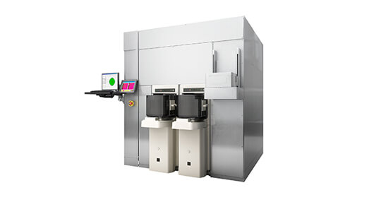
From SEMICON Japan comes the news of a large interposer stepper for 2.5D packaging applications just introduced to the market by USHIO, a Japanese manufacturer of light sources that also dabbles in developing products that contain it’s light sources. Based on its large-field stepper system for 2.5D/3D packaging released this fall, the company claims that this next-gen system will allow for interposer design flexibility and a significant reduction in manufacturing cost due to a number of features:
- It can process 405mm×350mm interposer substrates as well as 300mm silicon wafers.
- It is suited for interposers made of materials other than silicon, including glass and organic materials.
- It’s large-diameter projection lens enables throughputs of 120 wafers per hour.
According to the company, shipment of the system will begin in March 2013. In the mean time, you can learn more about it here, and see it on display at USHIO booth No. 4C-704. The company will also hold a release presentation and an exhibitor seminar at 11:00–11:20 on December 6 and at 12:30–13:20 on December 6 and 13:30–14:20 on December 7.
From the world of programmable FPGA’s, Max Maxfield of All Programmable Planet had some exciting news to share about Xilinx Virtex-7 2000T (you know, the poster child for 2.5D interposer technology that started shipping in October 2011?) Apparently, its 6.8 billion transistors, which providing designers with access to 2 million logic cells makes it the world’s “highest capacity programmable logic device.” It also makes it perfect for ASIC prototyping applications, and as a result is now powering Synopsys’ HAPS prototyping solution. Max had quite a discussion about it with Mick Posner, director of product marketing at Synopsys. You can read his post here.
Silicon Valley start-up, MonolithiIC 3D, sure seems to be stockpiling those monolithic 3D IC patents, adding a 20th to its list of granted earlier this week. The company reports that its 3D IP portfolio now covers logic devices, memory devices such as NV, NAND, R-RAM and DRAM, and electro-optic derivatives such as micro-displays and multi-spectrum imaging, and was also granted broad coverage for its wafer-scale-integration technology. In addition to 17 issued and 3 granted patents, the company says it has more than 50 patents pending, making it one of the key players in the 3D IC field.

With NAND Flash in particular, there’s been movement to manufacture NV memory using polycrystalline structures. Alternatively, MonolithIC 3D has been touting its monocrystalline technology, which they claim offers an even better foundation for monolithic 3D NAND, and empowers older wafer fabs to offer competitive new products and advanced fabs a longer effective manufacturing road map. The full press release is available here, and a great interview with Zvi Or-Bach, MonolithIC’s CEO, focusing on the company’s proposed paradigm shift for the semiconductor industry was recently posted on Pradeep Chakraborty’s blog.


