
I’ve come across a few interesting announcements in the 3D space today that separately are just random bits of news, but when bundled together, demonstrate acceleration to 3D commercialization. When you think about it, we’re more than halfway to Q1 2013, which has been earmarked by Micron as when 2 versions of its Hybrid Memory Cube (HMC) will roll.
Progress with the Hybrid Memory Cube Since the Hybrid Memory Cube Consortium was formed less than a year ago (October, 2011) by Micron and Samsung with the purpose of develop an open interface specification for a combination 3-D DRAM/logic device based on through-silicon-via (TSV) technology, it’s membership has expanded to include Altera, ARM, Hewlett-Packard, IBM, Microsoft, Open-Silicon, SK Hynix and Xilinx. Today’s news came to me by way of a post by Rick Merritt on EETimes, in which he reports that the HMCC released TO ITS MEMBERS, a draft of interface specifications. Merritt couldn’t report exactly on what the draft specs are about, because they are not shared publically until the HMCC members have had a chance to review and add input. He did report about previously publically released specs for an interface protocol and a short-reach physical layer channel. So here’s the key message: if your company wants to have input on the specs, it needs to become a member of HMMC. The organization is still accepting new members. You can find out more about that here.
More Temporary Bond/Debond Solutions
I’m glad Phil Garrou found time to write about the SUSS Workshop at SEMICON West, because I was only able to attend part of the event, and thus only reported on what the representatives from Yole, Imec and Ga Tech had to report. But about halfway down this week’s post on Insights from the Leading Edge, Garrou talks about three new temporary bonding solutions SUSS MicroTec is helping to develop with material suppliers Dow Corning, Dow Chemical, and 3M. Dow Corning’s is a silicone based bi-layer process that features a room-temperature debond step. Dow Chemical’s offering is BCB-based, and involves a cure step followed by a mechanical room temp debond step.
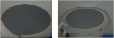 Dow Chemical’s carrier wafer on the left, and the cleanly debonded active wafer on the right. (courtesy, Dow Chemical)
 3M has two processes in the pipeline. The first improves upon its LTHC process by adding a high-temp thermoplastic prime layer to conventional materials to add a bonding surface for the UV curable adhesive and requires laser degradation for release. The second one “replaces the LTHC layer with a 100% solids UV curable “release layer” that is tuned to enable mechanical separation of the carrier at the interface,” writes Garrou For a more detailed explanation of the processes complete with diagrams, follow the link above.
It’s great to see so many new developments in the temporary bond/debond space as it has been earmarked as one of the remaining challenges to 3DIC commercialization.

OSATS Increase Capex for 2012 in Anticipation of 3D ICs
According to a news item posted on Digitimes, titled Major IC Packagers Step up 2012 Capex, the top 3 OSATS (ASE, Amkor and SPIL) have all increased their 2012 capex budgets mostly to expand capacity for high-end advanced packaging processes including wafer-level, copper pillar bumping, and TSVs and other 3D IC packaging. Of the 3, ASE disclosed that 30% of its investment will be targeted for flip chip packaging. If you’re a person who likes to see detailed numbers and percentages, I suggest reading the full post. ~ F.v.T.


