
As chip-to-wafer (C2W) stacking has been identified by most technologists as the best approach to 3D stacking for optimum yields and the ability to stack dies of different sizes — especially in memory/logic stacks — a number of approaches have been or are being developed by various collaboratives. At IMAPS Device Packaging, held March 8-10, 2011 in Scottsdale AZ, two approaches were presented by Dan Pasqual of SEMATECH and Gilbert LeCarpentier of SET, respectively. I talked to them about the projects they were involved in, and also touched base with Thorsten Matthias, of EV Group to compare these with the work EVG has been doing with Datacon and learn about their involvement in the others. Additionally, I interviewed Leti’s Mark Scannell and Thomas Signamarcheix to get an update on the PROCEED project.
Tacking Material…..
According to Pasqual, the priority and focus of SEMATECH’s work is feasibility of bond using a novel thermo-decomposable tack material for the pick-and-place step. The concern they are addressing is with organic materials that stay in the process, and the subsequent outgassing issues with copper bonding. The goal is to maintain the achieved accuracy of 2.5µm with a misalignment of less than 1µm through collective bond step with a polymer material that didn’t interfere with the copper bond. Speed of processes is not part of this work.
SEMATECH’s two-step process begins with a handle wafer on which a 50µm TSV wafer that’s already been through backside processing is mounted. A thermo-decomposable adhesive is spin-coated on the wafer. This sacrificial material maintains alignment through the collective bond. Using die bonder, die are tacked to the wafer’s surface using a fast tacking cycle. This material becomes sacrificial, evaporating during the collective thermocompression bond.
The primary differentiator between SEMATECH’s collective bond process and the work being done in at IMEC and by EVG and Datacon is the tack material. IMEC uses a photo-patternable adhesive that becomes underfill when used with a copper nail interconnect, explained LeCarpentier. While EVG also uses a sacrificial evaporating adhesive material, the bake temperature is higher than that of SEMATECH’s, 250°C bake-out temperature. However, the focus of EVG/Datacon’s work is to develop a process for high volume manufacturing, rather than honing in on the tack material used. Matthias also pointed out in our discussion that the work being done at SEMATECH, IMEC and Leti is done using EVG bonders for the collective bond step.
…. Vs. Direct Bonding
Leti’s process is altogether different from the others, and uses a room temperature, direct metal or direct oxide bond as the first of a two-step process rather than an adhesive. The French research institute initially developed direct bonding for wafer-to-wafer (W2W) bonding, and has adapted it for C2W bonding because C2W has been identified as the trend for 3D integration.
“We like the metal-to-metal bond because it occurs before thermal treatment, so there is no play when the die attached, resulting in better alignment accuracy and the potential for higher density,” explained Scannell,” You don’t have to design in room for play.” Additionally, he said the short bonding time should lead to higher throughput. Another benefit is that rather than forming the physical bond in the second step, it is actually formed through that first direct bond process. Annealing only serves to initiate the recrystallization process, explained Scannell.

How to PROCEED
The greatest challenge with this approach, according to LeCarpentier, is that it requires a die bonder that could handle clean processes. Additionally, in the first step oxide must be removed from the copper. The SET FC300 is typically not a clean machine, he explained. Direct die bonding needs very clean surface. Enter the PROCEED Minalogic project a 4.2 million-euro, 24-month project that began in December 2009, is supported by French FIU (Fond Interministeriel Unique) and includes Leti SET, STMicroelectronics, ALES and the CNRS-CEMES.
As a partner in the project, SET was charged with customizing a tool to demonstrate the process (Figure 1). LeCarpentier said adaptation involved changing some material used internally, changing how cables are arranged, added protection to avoid falling particles, and controlled air flow through the machine to minimize contamination. ALES contribution to the project is plasma preparation and pre-clean of the copper surface. ST Mirco is working on the demonstrators, developing requirements to achieve cleanliness and planarity. LeCarpentier explained that the ultimate goal is to transfer the technology to high volume, and the tool for that is currently on SET’s roadmap.
Figure 1: Customized FC300 From SET.
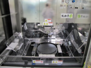 Figure 1: Customized FC300 From SET.
According to Signamarcheix , laboratory manager for PROCEED, says the goal is to complete the in 18-24 months to be current with the partners. It’s part of rolling development in different areas. The machine should be perfected for research needs by the end of the year. SET is developing a production level equivalent.


