
Sorry everybody, but I couldn’t resist this Buzzfeed-esque title, because Besi’s Hugo Pristauz’ unprecedented use of “colorful” language to illustrate the “turbulent plane ride” of ramping thermo-compression bonding die attach to volume production just might go down in history as the most talked (and laughed) about incident at the 2016 3D Architectures for Semiconductor Integration and Packaging (3D ASIP) Conference (December 13-15, Burlingame, CA). He did follow it up with the comment, “it has to be a repeatable process,” and I’m not one to disappoint, so I’m repeating it here! One thing is for sure, at 4 pm on the second day of presentations, it certainly did wake up the room! Of course, that wasn’t the only memorable moment from this three-day conference, now in its 13th year and under a new banner as part of the International Microelectronics and Packaging Society (IMAPS) for the first time.
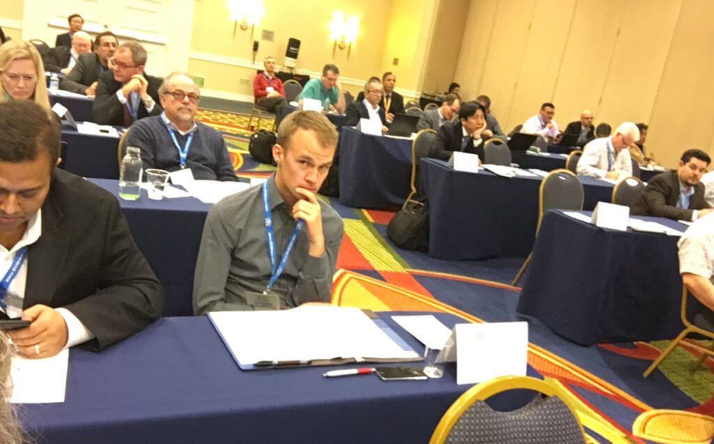
Overall, this was a very different event than the 12 previous versions. Once the reigning king of 3D integration conferences when 3D through silicon vias (TSVs) were the hottest thing since, well, flip-chip packaging; 3D ASIP has evolved considerably over the past few years as 3D becomes part of the overall advanced packaging landscape. This year’s event drew a dedicated yet intimate crowd of 3D enthusiasts who spent a great deal of time reminiscing about achievements of the past year, talking about the number of product roll-outs containing fan-out wafer level packaging (FOWLP), and setting the groundwork for the next big thing: setting a course for heterogeneous integration. As Bob Patti, Tezzaron explained to me, finding speakers with new stories to tell was a challenge because as 3D becomes commercialized, customers are very hush-hush about what they are doing. Next year, apparently, there will be lots more to tell.
In the past, sessions were dominated by suppliers talking about individual process steps from TSV fabrication through temporary bond/debond for backside processing, thinning, stacking, etc. Now, what’s new from the suppliers filled one session. The rest of the conference content focuses on key applications, alternative approaches, and the heterogeneous integration roadmap. The three most talked-about topics included CMOS Image sensors (CIS), hybrid bonding, and IP block reuse. For those of you who regularly read 3D InCites, much of this is not news to you. We’ve been following these stories for some time. Still, they bear repeating, and it’s good to have validation from the key players. Read on for the highlights.
CMOS image sensors
The flagship application is benefiting even more from 3D stacking technologies, enabling next generation functionalities. According to Sony’s Tetsuo Nomoto, the next step for 3D integration in CIS enables interconnections in the pixel area to add new functions. He showed a 3D stack that had the sensor array stacked on the analog-to-digital converter (ADC) die, on a memory die, on a processor to allow real-time image processing.
On Semiconductor’s Roger Panicacci echoed Nomoto’s statement, adding that applications are being driven by improved pixel performance in a number of markets including mobile, automotive, security, Internet of Things, and more.
Franz-Schrank, AMS AG said that 2.5D and 3D integration technologies are a prerequisite for cost-efficient, wafer-level packaging for opto-sensors. The company uses a tungsten-lined, TSV last approach rather than a Cu-filled, TSV-mid approach. Other key technologies included wafer bonding and die-to-wafer stacking.
“3D stacking is a major image sensor design breakthrough and will be a driving force for the next few years,” said Barmak Monsoorian, Forza Silicon.
Hybrid bonding [aka Tessera’s direct bond interconnect (DBI®)] was mentioned in almost every single presentation as a critical process for everything from next-generation 3D image sensors to memory stacks, to 3D systems on chip (SOCS). Paul Enquist, Tessera, has always known that hybrid bonding was the key to 3D stacking for Image sensors. How? It was his idea.
Enquist noted that DBI has become the de facto industry standard for CMOS image sensor volume manufacturing. Enquist explained how per pixel 3D interconnects are enabled by submicron scalable DBI, through the stacking of more than two active layers. At low temperatures, it achieves high bond energies for low bond distortion. Additionally, he said DBI cost and performance advantages is not limited to CIS. It is universally realizable for 3D SoC and 3D Memory. “Paul, you developed this, and now it’s how part of the 3D industry will move forward,” said Phil Garrou, introducing Enquist. “Congratulations. You stood behind what you were doing, and It’s now being used by all the big boys in the industry.”
IP Block Reuse
Subu Iyer, UCLA’s CHIPS; Tim Olson, Deca Technologies; Patrick Soheili, eSilicon; Tim Lee, Boeing; and Denis Dutoit, CEA-Leti, all talked about the benefits of IP reuse in “chiplet” or “dielet” form integrated on and “interconnect fabric” for a low-cost, multi-functional, 3D SOC solution.
At CHIPS, Iyer’s team is working with off-the-shelf IP blocks that are interconnected on silicon. What makes these SuperCHIPS so cool? Three things: they are non-proprietary, used all the time in SoCs, and are easy to implement.
Deca’s Tim Olson talked about a similar approach he referred to as Fan-out (FO) SoC. What differentiates fan-out SiP from fan-out SoC? The former uses chips that were designed to be stand-alone and are packaged together. FO SoC refers to a group of disparate semiconductor functional blocks embedded within an organic material upon which electronic interconnect or fan-out fabric, is created to connect the blocks and create a virtual SoC.

Deca’s secret sauce to high yields enabling FO SoC is its proprietary adaptive patterning/adaptive alignment processes, which resolves the die shift problem by aligning RDL pattern to the measured die position. It enables high metal density designs and precisely aligns inductors to the die. So you know that turbulent plane ride of thermo-compression bonding for die attach we talked about earlier? Olson referenced that saying, “Hugo, we don’t need to take that ride with adaptive patterning.”
Heterogeneous Integration
Rich Rice, ASE, noted that while semiconductor growth over the next few years is forecasted to be in the single digits, the growth we will see will be in the 2.5D heterogeneous integration space, with system-in-package (SiP) as a key enabler because it has many drivers, one of which is miniaturization. “Moore’s law is less accessible, not dying,” he said. “I don’t profess to know what will happen in the future, but economically it’s less accessible for everyone. This is where packaging will have its play.”
ASE’s Bill Chen talked about reinventing the technology roadmap with the recently introduced heterogeneous integration roadmap. “One thing that hasn’t changed (over the past 20 years) are the number of people who talk about the end of Moore’s Law,” he joked. According to one Microsoft executive that he heard speak recently, Chen reports that “the number of people who talk about the end of Moore’s Law will double every year.”
In all seriousness, Chen noted that there are still believers in Moore’s law. 7nm devices have been realized technology-wise, that shows we are continuing to advance along Moore. Chip design cost escalation is the real issue, and how will we deliver this design and still make money. “Now it’s not enough to deliver a piece of silicon. We have to offer complex solutions at a large scale,” he said. Companies have to do something different than they’ve done before.
Chen noted that even Gordon Moore talked about this in 1965, and quoted Moore as saying “It may prove to be more economical to build a large system.”
Subu Iyer, who heads up UCLA’s Center for Heterogeneous Integration and Performance Scaling (CHIPS), concurred. “Innovation cannot happen in our industry unless it is democratized. What’s happening in the industry today is that the barrier to entry is so large, only 2-3 companies can build silicon, and only 2 or three may soon be able to design it,” he said. “We can’t scale ourselves out of the power gap. Heterogeneous integration solves the interconnect density problem.”
Final thoughts on 2.5D and 3D vs. Scaling:
“Until there is an atomic shrink ray to shrink the size of atoms, 2.5 and 3D is going to be the way forward,” said Bob Patti, of Tezzaron and also now Nhanced Semiconductors, Inc. He called interconnect “the root of all evil” and noted that TSVs enable shorter wires so we can do “neat things” with 2.5D and 3D.
“We aren’t killing SoC with multi-die integration – we are giving them an opportunity as building blocks in advanced packages,” noted Herb Reiter, eda2asic.
That’s it for now. Look for more coverage of 3D ASIP from Herb Reiter and Paul Werbaneth after the holidays! ~ F.v.T


What were the key technical aspects of Pristauz’s presentation that backed up his frustration with TC FC ?
Was there any presentation ( Enquist ? ) / discussion on the merits of continuing with TC FC bond vs shifting to DBI for 3d stacks ?
Dev,
Pristauz said that TCB core capabilities of accuracy, coplanarity, and bond control are needed to achieve current HVM requirements of 99.8% yield. Besi is building a tool for 5µm pitch, with a goal of reaching 2-10µm pitch in the future. The biggest challenge is coplanarity integrity that is essential to ramp these processes to HVM.
I do not recall anyone specifically recommending continuing with TC FB bond vs. shifting to hybrid bonding. Hybrid bond was always discussed as the enabling technology for next-gen applications, from image sensors, to memory, to 3D SoC stacks. I hope that answers your questions. The proceedings have not been shared at this point.
FvT :
Thank you, Frohe Weihnachten
Herr Pristauz’s concerns with in situ TC FC bond are not new. We had to solve those and more in the first application of this variation of FC when we invented it at Moto ( SPS ) and put it into HVM back in 1995 at a Robotic Line in Tempe for GaAs PAs
There needs to be more in depth R&D to make TC FC painless for 3d stacks.
dear Dev, thanks for your interest. One of my key points in my presentation is that we need a good understandig of the core capabilities of a TC bonder which are accuracy and co-planarity if we want to walk down the pitch roadmap down to 1 micron on C2x based using TC-bonder. With TC bonding we run into the issues that come with the rapid temperature ramp which comes with considerable challenges for the accuracy and the co-planarity integrity during the ramp. Even I see possibilities to walk down the pitch roadmap with TCB I think the process will stay slow and comes with major challenges.
My personal thinking is that DBI (or hybrid bonding) is the right way to go down this pitch roadmap. You’re tacking the die cold and anneal the bonds in a batch process. You get rid of the temperature ramping, and the price you pay is the requirement to be super clean. But to make a clean machine seems to be much easier than managing all the challenges for sub-micron accuracy that come with the (f-bomb) temperature ramp. Without temperature ramp I think building a bonder with 100-200nm accuracy and a throughput of 10.000 to 20.000 UPH is not too difficult.