


Reflections on My Year as the 3D InCites Editorial Intern
Over the past year, my role as the 3D InCites editorial intern has given me a front-row seat to one of the most dynamic corners of the semiconductor world: advanced packaging and heterogeneous integration. My duties spanned writing Member Monthly News, creating LinkedIn content, contributing feature articles, and even representing...
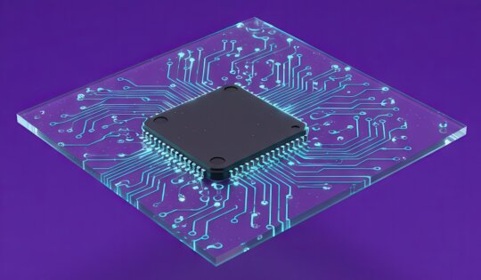
Is Copper Sintering the Key to Advancing Wide Band Gap Semiconductors?
By Rejoy Surendran and Xinpei Cao, Henkel Adhesive Technologies In the mid- to high-voltage power semiconductor sector, which enables EVs, telecom networks, energy infrastructure, and industrial innovation, wide band gap (WBG) semiconductors like gallium nitride (GaN) and silicon carbide (SiC) are on their way to surpassing silicon (Si) for power...

IFTLE 649: Let the Hybrid Bonding Wars Begin! Also: Samsung Locks in Glass Interposer Source
Adeia vs AMD Hybrid bonding is a semiconductor packaging technique that enables direct Cu-Cu and oxide-to-oxide connections, eliminating the connection using microbumps. This approach improves interconnect density, electrical performance, and thermal efficiency, making it an important advanced packaging technology for next-generation semiconductor devices. Adeia Semiconductor Solutions, a wholly owned subsidiary...
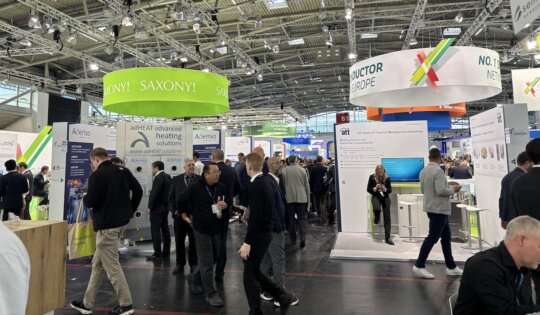
The EU’s Semiconductor Strategy: CHIPS Act 2.0, Investments, and More
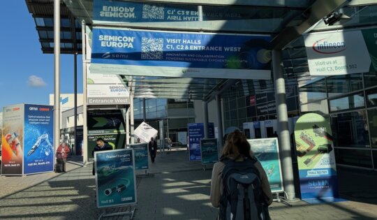
I recently attended SEMICON Europa in Germany to learn how the EU is approaching the next phase of its semiconductor development. From what I learned, the EU is moving its industry forward by planning for its CHIPS Act 2.0 legislation, attracting new investments, and funding competitive R&D pilot programs. In...
November Member News: Shaping the Future of Semiconductors
November was a dynamic month for the 3D InCites community and the broader semiconductor industry, with companies showcasing innovative technologies, celebrating leadership achievements, expanding global operations, and advancing workforce development. From product launches and AI‑enhanced design platforms to award recognitions and strategic partnerships, industry leaders highlighted breakthroughs in advanced packaging, inspection,...
IFTLE 648: Unimicron Glass Core Substrates and Hybrid Bonding
With all the hype surrounding the potential use of glass interposer substrates and hybrid bonding, I thought taking a deep dive look at the recent publication “Flip Chip on Glass Core Substrates with Microbump and Cu-Cu Hybrid Bonding” ,which appeared in the IMAPS Journal of Microelectronics and Electronic Packaging, by...

Co-Packaged Optics: Today’s Biggest Packaging Push
Co-packaged optics is one of the most talked about innovations in advanced packaging right now, and it’s for good reason. It promises higher bandwidth density, lower power consumption, and reduced latency over other packaging approaches – all of which are essential for enabling smarter AI solutions. To learn more about...
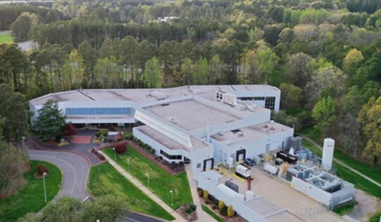
IFTLE 647: Micross AIT on Track to Deliver 300mm Bumping Onshore
Continuing our look at program information deemed “OK for public release” at the recent IMAPS Onshoring conference, let’s examine what Micross had to say about progress on its Re-shore Ecosystem for Secure Heterogeneous Advanced Packaged Electronics (RESHAPE) 300mm bumping line, sponsored by DARPA’s Industrial Base Analysis and Sustainment (IBAS) program....
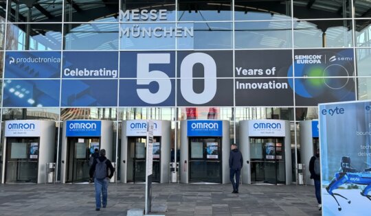
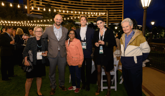
Passing the Torch: Reflections from SEMICON Europa 2025
While announcing my retirement after 20 years in the industry at IMAPS Symposium brought my career in advanced packaging full circle, wrapping up my 3D InCites career at SEMICON Europa brought closure. It was at SEMICON Europa 2007, held in Stuttgart, where my fascination with 3D integration and packaging first...

IFTLE 646: TSMC 3Dblox 2.0 Helps Advanced Packaging Designs
The 3Dblox Open Standard Continues to Evolve Introduced in 2022, the 3Dblox open standard has provided EDA vendors with a pathway to model the essential physical stacking and logical connectivity information for 3D IC designs in a single format. 3Dblox reportedly simplifies 3D IC design by providing a complete view...
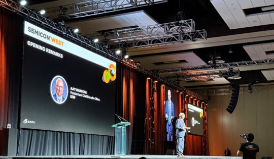
SEMICON West Navigates Semiconductor Industry Changes
As Benjimen Franklin said, shortly after the US Constitution was written, “In this world, nothing can be said to be certain, except death and taxes.” I’ll add one comment to that: Change. Change is constant. Over the past year, there has been a significant amount of change in the semiconductor...

From Reactive to Proactive: Semiconductor Shipment Visibility in 2025 and Beyond
In 2024, electronics cargo theft, including semiconductors, servers, and high-end computing equipment, surged dramatically, exposing a critical vulnerability in supply chains. ¹ This threat is not just a security issue for companies shipping semiconductors and other high-tech components; it directly impacts revenue, causes production delays, and compromises customer trust. Often,...
Advanced Packaging: A Community Coming Together
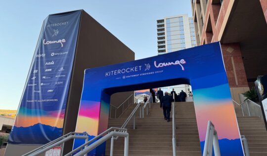
In the past 16 years, 3D InCites has watched the 3D packaging industry grow. The philosophy of 3D InCites was to create an advanced packaging community. At SEMICON West in Phoenix, the community was out in force, from ribbon-cutting ceremonies for new facilities, to new packaging equipment companies showing for...

Jessica Yang: My Summer Internship at Saras Micro Devices
By Jessica Yang, HR Intern, Saras Micro Devices Hi, I’m Jessica Yang, a rising junior at Washington University in St. Louis, studying Organizational & Strategic Management and Sociology. With my two interests, I’ve always been passionate about the people side of business, which is why I was looking for internships...

IFTLE 645: ASE Packaging in Koahsiung; Amkor Advanced Packaging in AZ; US-SMC?
ASE to build new packaging facility in Kaohsiung Taipei Times reports that ASE, the world’s biggest chip assembly and testing service provider, said it is investing $578.6M to build a new advanced chip packaging facility in Kaohsiung to cope with fast-growing demand from artificial intelligence (AI), high-performance-computing (HPC) and automotive...
Henrik Ng: My Summer Internship at Saras Micro Devices
My name is Henrik Ng and I am an Electrical Engineering student entering my junior year at Georgia Tech. I was eager to gain both hands-on experiences and theoretical understandings in the realms of RF engineering, as inspired by my previous research project surrounding RFID energy harvesting. At the same...

Will AI Ever Become Profitable?
Last year, I wrote a blog on the growth of AI, where I broke down the public hype around the technology and the barriers preventing it from scaling further. Earlier this year, Gartner projected that worldwide AI spending will reach $1.5 trillion by the end of 2025, up $490 billion...
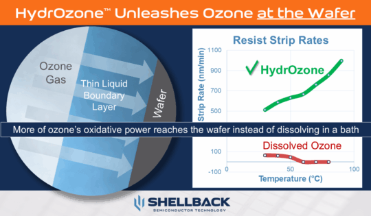
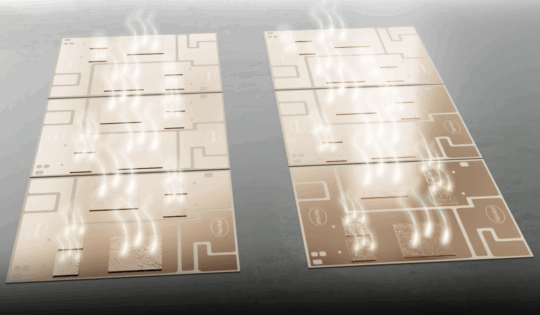
Product-Proven Green Alternative to Solvent and Piranha Wafer Processing using Ozone
The use of ozone in semiconductor wet processing surface preparation has gained new momentum as fabs pursue advanced cleans and strip steps that reduce chemical waste without compromising performance. In theory, ozone’s oxidation potential (2.07 V) makes it one of the strongest practical oxidizers — far exceeding hydrogen peroxide or sulfuric...

October Member News: Shaping a Smarter, More Connected Semiconductor Future
October proved to be a dynamic month across the semiconductor and advanced packaging ecosystem, marked by innovation, expansion, and global collaboration. From groundbreaking facility announcements and strategic partnerships to prestigious industry recognitions, members continued to push technological and manufacturing boundaries. The month also featured major events, where companies unveiled cutting-edge...
SEMICON Europa 2025 Member Preview
As many of you know, this year’s SEMICON Europa in Munich is a special one for 3D InCites. The Queen of 3D is retiring, and SEMICON Europa marks her last industry event. Over the course of her career, she has played an instrumental role in the advanced packaging industry. From...