


The Telecom Network Semiconductor Trifecta
Telecommunication networks are undergoing a rapid transformation. With 5G rollouts, edge computing, and a surge in IoT devices, the pressure on semiconductor performance is higher than ever. But today’s chipmakers aren’t just racing to deliver speed and power—they’re also being challenged to meet complex regulatory requirements and ambitious sustainability goals....
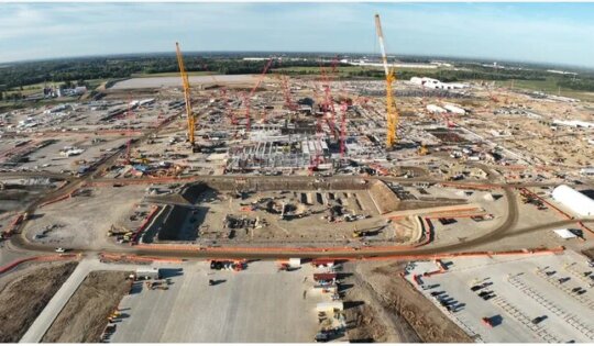
IFTLE 640: Intel Ohio in Limbo; US Government Acquires 10% Stake in Intel
Intel Ohio is started, but when will it be finished? The Columbus Ohio Dispatch has just reported that Intel is still committed to its proposed Ohio production facility, but it will “further slow down” construction at its future Ohio microchip factory. Intel announced this slowdown July 24 during its second...

Allen Mai: My Summer Internship at Saras Micro Devices
Hi, I’m Allen Mai, a senior studying Computer Science at Georgia Tech. I found Saras Micro Devices on LinkedIn and was immediately drawn to the startup environment. I had a great experience working on a startup-style team during my junior-year capstone, and I wanted to re-engage with that fast-paced, collaborative...
Revolutionizing Semiconductor Quality: The Dynamic Planar CT Advantage
X-Ray inspection has become an essential component in semiconductor manufacturing, with 3D imaging emerging as a critical tool for ensuring product quality and reliability. In a recent discussion with Andrew Mathers, Principal Product Line Manager at Nordson Test and Inspection, we gained valuable insights into how advancements in 3D x-ray...

IMAPS Symposium Member Preview 2025
The IMAPS Symposium is just around the corner! Taking place from September 29 through October 2 at the Town & Country Resort in San Diego, California, this year’s event will emphasize advanced packaging structures, advanced interconnects, bumping and wire bond technologies, MEMS and sensors, RF, and more. With 18 of...

Risk Mitigation in Semiconductor Capital Equipment Logistics 2025
Discover the key challenges in semiconductor capital equipment logistics—and how to build a proactive, flexible, and future-ready supply chain that prioritises safety, security, and minimal handling Interview with Barry O’Dowd, Senior Vice President, Global Head of Business Development for Semiconductors Q: What are the main logistics challenges when moving fab...

August Member News: Pivotal Shifts in Leadership, Investments and Innovation
The month of August held pivotal shifts in the semiconductor industry, marked by leadership transitions, targeted investments, and continued innovation across packaging, inspection, and AI-enabled design tools. Companies introduced advanced process solutions and new product lines at global events, underscoring the sector’s push toward higher reliability, efficiency, and scalability in...
IFTLE 639: Are Things Worsening for Intel? Will Samsung Add Advanced Packaging in Texas?
Intel Concerns Continue to Grow Long time readers of IFTLE know that we have been following the technical and financial issues recently plaguing Intel. Recent reports in Reuters and EE Times have pointed out some added concerns. EE Times notes that former Intel CEO Pat Gelsinger poured billions of dollars...

The Unfinished Revolution for Advanced Packaging and Heterogeneous Integration
Amazing breakthroughs lie ahead. It won’t be easy — but it will be awesome. How it started I remember when wafer-level stacking was brand new. It wasn’t “advanced packaging” back then. Even the term “3DIC” was brand new. The idea was audacious and stunning and we loved it. We seized...
IFTLE 638: TSMC Advanced Packaging Coming to AZ; Intel Stops Internal Glass Core Substrate Funding
TSMC Advanced Packaging in US Scheduled for 2028; Focusing on SoIC/CoPoS From Taiwan we hear that TSMC has accelerated Fab construction in Arizona. The third wafer fab in the United States will use N2 (2nm) and A16 process technology. It has been reported that equipment manufacturers were notified of this...
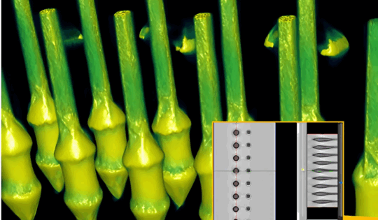
Copper Dual Damascene for Wafer-Level Packaging: Enabling Reliable, High-Density Interconnects
Overcoming yield loss, reliability risks, and scaling limits in advanced packaging with high-aspect-ratio copper interconnects. As device architectures shrink, delivering high-reliability, fine-feature interconnects without sacrificing yield or performance has become a critical challenge for semiconductor manufacturers. In fan-out-wafer-level-packaging (FOWLP), chiplet-based designs, and high-density 2.5D/3D integration, the need for compact, high-performance...
SEMICON Taiwan 2025 Member Preview
Are you ready for an exciting week at SEMICON Taiwan 2025? From September 8-12, more than 1,100 semiconductor companies from around the world will gather at the Taipei Nangang Exhibition Center to network, share insights, and plan for the future. As the industry gets closer to reaching its $1 trillion...

Can We Make Data Centers Less Power Hungry?
When the headline reads “Power Usage in Wyoming data center could eclipse consumption if the state’s human residents by 5x, the tenant of colossal investment remains a mystery.“ It grabs your attention. The article goes on to discuss that the data center is expected to start at 1.8 gigawatts and...

Reducing Greenhouse Gas Emissions Starts with Raw Materials
Everybody’s talking about reaching net-zero greenhouse gas emissions, but what does this actually entail? According to Pierre Farbos de Luzan, Henkel’s head of sustainability for electronics adhesives, the road to net-zero starts with raw materials. To understand why, it’s important to touch on the different emission tiers – Scope 1,...

Sustainability 101: Carbon Credits – Definitions and Directions
If your company is committed to achieving net zero carbon emissions, meeting that commitment will require purchasing carbon credits. Although the first steps should be to reduce your Scope 1 and Scope 2 greenhouse gas emissions as much as possible, a manufacturing facility cannot get to zero without some offsetting....

IFTLE 637: UMC Re-Enters the Advanced Chip and Advanced Packaging Markets
According to Nikkei Asia, UMC is eyeing 6nm production, with a focus on chips for Wi-Fi, RF, Bluetooth, AI accelerators, and processors used in TVs and vehicles. In 2017, UMC began to focus on mature process nodes rather than competing at leading-edge technologies dominated by TSMC. This allowed UMC to...

An Inside-out-view: Data Centers
The convergence and synergy of performance and sustainability required to power the next generation of AI data centers The surging demand for AI data centers is transforming the semiconductor industry, redefining chip design and manufacturing priorities. According to McKinsey, AI-ready data center capacity is expected to grow at a 33%...

Managing Security and Access of Semiconductor Manufacturing’s Remote Connectivity
In the complex world of semiconductor manufacturing, equipment uptime is critical to productivity. Modern industrial operations are no longer limited by physical boundaries. When issues arise, quick resolution is essential, a unique challenge with global supply chains and specialized expertise scattered across continents. Rapid advancements in Industrial IoT (IIoT) make...

IFTLE 636: Samsung’s Approach to Silicon Bridges; Micron HBM Packaging Planned for Virginia
ECTC 2025 The 75th annual IEEE Electronic Components and Technology Conference (ECTC), was held this year in Dallas TX over memorial day week. It featured: 2,500+ attendees 390 technical papers presented in 36 oral and 5 interactive presentation sessions. 16 professional development courses Industry support included 51 corporate sponsors and...

Meeting the Cleaning Challenges of High-density 3D Heterogeneous Integration Applications
Today’s rapid growth in 3D heterogeneous integration (3D HI) is being driven by a plethora of high-performance computing applications driving the microelectronics industry, including autonomous driving and artificial intelligence. This strong need for 3D HI has pushed capital expenditures for advanced packaging at a remarkable pace. The advanced packaging market...