We all know how important inspection is for advanced packaging. Not only are these processes critical for ensuring higher yield, but they’re also integral for maintaining device reliability. As the industry pushes for smaller features and tighter spacing, even the smallest defects can pose major challenges. For instance, delaminations and air gaps can be detrimental in a market that demands increasingly complex devices. Such defects will lead to electrical or mechanical failures down the road.
One technology that’s mitigating these issues is acoustic micro imaging (AMI). AMI is a high-frequency ultrasound technology, and it’s being used by the industry as an inspection method.
How AMI Works
To learn more about AMI and its role in advanced packaging, I spoke with Rebecca McCordic, senior application engineer at Nordson Test & Inspection.
McCordic explained that at the core of AMI technology is a transducer, or a device that turns energy from one form to another. It starts with a pulse of electrical energy, then converts it to mechanical energy, or a high-frequency ultrasound wave. Because ultrasound doesn’t travel through air, this allows inspectors to obtain clear images of gaps and delaminations in the device that could otherwise be difficult to see.
However, the transducers used for AMI are not all the same. Each transducer handles a specific frequency, and they’re chosen based on the sample that needs to be inspected. By moving the transducer across the sample, the inspector can generate multiple images that can then be analyzed by the AMI software. Through this analysis, the inspector can choose to accept or reject parts based on the number of defects the package is found to have.
So, how do these defects typically present themselves?
The biggest difference between ideal and defective samples, McCordic shared, is that some defective samples will have very clear air gaps. However, another common defect McCordic noted is thinning of the attach material on solder pads. When this material is too thin, any stress that would be put on the device could lead to delamination. An uneven solder or thermal interface material (TIM) layer may also indicate a larger problem with the build process.
When to Use AMI – Inspection, Destructive Testing, and X-rays
With the ability to gather so much information without damaging the device, I also asked McCordic why anyone would choose to perform a destructive test to identify a defect, rather than simply use AMI inspection to check for them. One reason, she explained, is for R&D purposes. Oftentimes, companies want to ensure that a process is fully developed before integrating it into their production cycle, and a destructive test can confirm proof of concept for AMI.
An example of this in action is a standard capacitor inspection. New capacitor companies will often require a destructive test to confirm the presence of voids or delaminations found by the AMI software. Once the destructive, proof of concept has been completed, the company can then integrate the software into their inspection process.
McCordic also highlighted some of the key differences between AMI and its transmission technology counterpart, which is more comparable to X-ray. Whereas AMI is an ultrasound technology, transmission scanning uses both a sending and receiving transducer positioned above and below the sample. Both transmission technology and X-ray create composite images, unlike AMI, which inspects layer-by-layer.
“Ultrasound and X-ray are complementary technologies,” said McCordic. “There are some things AMI can do that X-ray can’t, and vice versa.”
For certain applications, McCordic noted that both technologies may be recommended. For example, composite images are preferable for inspecting spherical objects like ball grid arrays.

The Challenges and Future of AMI
Although AMI technology has tangible benefits, keeping up with the industry’s rapid pace is a hurdle that AMI must continually overcome. As applications become more complex, AMI software needs to quickly adapt to changing components. For instance, instead of scanning a single flip chip, AMI software could now be required to inspect multi-die stacks.
One way this mounting complexity is being addressed is through machine learning algorithms.
For example, some wafers have via patterns that look similar or identical to delamination, and humans have typically been responsible for distinguishing them. However, McCordic explained that through advancements in machine learning, AMI software can now identify via patterns and exclude those from the defect count. As machine learning becomes more robust, it will open new doors for inspecting increasingly complicated devices.
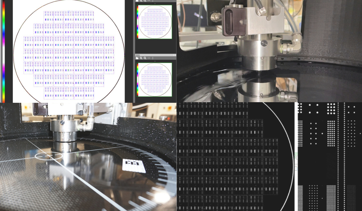
In addition, customer requirements for higher resolution and better throughput are also driving new developments for AMI software. To meet these rising demands, Nordson Test & Inspection developed its automated SpinSAM tool that can inspect four, 300mm wafers at a time.
“The wafer motion itself is revolutionary, because we’re spinning the wafers to get a higher throughput,” said McCordic. “It’s a huge improvement over systems from the past.”
Traditionally, acoustic microscopy systems move the transducer in a raster pattern, which is a small grid made up of individual pixels. This approach allows inspectors to collect data at every XY point, but it also requires decelerating to turn the transducer at the end of each line, thereby reducing throughput. Some acoustic microscopes address the need for better throughput by skipping lines and interpolating data points, or by using multiple transducers and stitching images together – both of which have their own drawbacks.
In contrast, SpinSAM spins the wafer to move the transducer and the wafer continuously, allowing inspectors to scan each pixel faster, allowing for better throughput without image stitching distortion.
Learn more about Nordson Test & Inspection and its new AMI SpinSAM solution.