

By Ming Zhang, Ph.D., Vice President of Fabless Solutions
While AI has made significant inroads in semiconductor design and manufacturing, semiconductor test is “the next frontier,” a bridge between design and manufacturing that resolves blurry boundaries between traditionally separated domains.
More specifically, by connecting design and manufacturing, tests help product and chip companies make better and cheaper products faster. As the boundary between these domains becomes increasingly less obvious—especially with advanced packaging and heterogeneous integration—testing provides essential validation and feedback to how products are architected and designed.
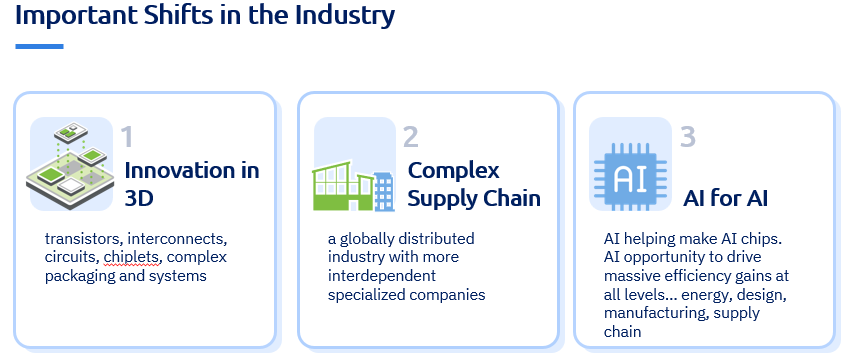
Using AI for innovation in semiconductor test will offer the ability to share real data that inevitably relates to yield, coverage and cost. It comes down to three trends highlighting these challenges—3D innovation, globally distributed supply chain and AI for AI.
Innovation in 3D in terms of three-dimensional transistors such as Gate All Around or 3D interconnect, 3D stacking of chiplets. In effect, the chip system is becoming a subsystem.
The supply chain is becoming more globally distributed, driven by technical factors. Fundamentally, integration or heterogeneous integration requires a global distributed supply chain from substrates to chiplets to resistors, services and fabrications. The challenge also includes a geopolitical aspect.
“AI for AI” with demand for AI technology is coming from the consumer world. The fact that AI has developed further due to more capable chips and better algorithms is making it easier to use AI where AI is produced—semiconductor manufacturing and testing.
Advanced and flexible testing strategies will be crucial to meet growing demand for chip performance and reliability and the bridge between design and manufacturing.
The Unique Challenges of AI for Semiconductor Testing
Applying AI to semiconductor testing is quickly changing the landscape as we know it, offering up both technical challenges and innovation opportunities.
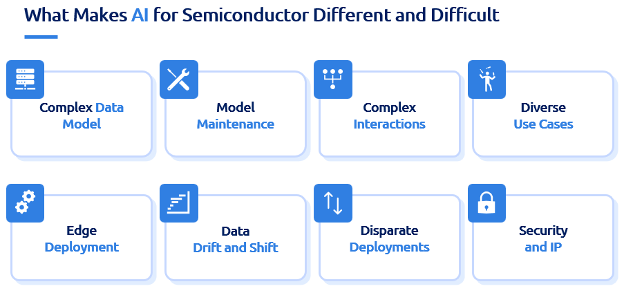
Several factors make AI applications in semiconductor testing particularly challenging, starting with complex, heterogeneous data. Test data comes in various formats—parametric readings, pass/fail results, images—from multiple sources. Diverse use cases such as binning and chiplet matching demanding cost reduction and quality enhancement can create a range of challenges, as can model maintenance requirements as high stakes for errors demand constant monitoring and adaptation.
Complex deployment scenarios about edge, server or cloud implementations can affect responsiveness while security concerns cannot be overlooked because semiconductor test data is highly sensitive and proprietary. Advanced packaging adds another layer of complexity, requiring tracking of individual dies from multiple wafers, along with discrete components from various sources.
Several promising applications for AI in the test space have the potential to solve at least some of these challenges. They include adaptive testing to modify test processes based on upstream results and system binning, matching chiplets with similar behaviors for optimal performance. Predictive binning could identify potential failures early to save downstream costs. System-level testing (SLT) to balance comprehensive testing with cost constraints is also gaining in popularity.
Some real-world data from a test-time reduction example shows the promise of AI for test. By using machine learning (ML) to predict which components would pass final testing based on earlier test results, some selective tests could be omitted, reducing costs while managing quality impact. That ML solutions won’t be 100% perfect—some tests showed zero escapes after ML implementation, while others showed finite defect rates. Similarly, ML isn’t useful for all chips—its utility varies by test and product characteristics.

Challenges Remain
Further exploration needs to be done for manufacturing across the complex and distributed supply chain to create effective monitoring systems. It should start small to learn from limited data sampling to determine when to stop modeling and start inferring, especially for low-volume products. Cross-factory and cross-design learning is a must-have requirement for transferring AI models between products and the manufacturing site. Finally, balancing AI and human expertise will help find the right combination of automated and human-guided decision making.
The Path Forward
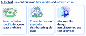
AI for test is the next frontier of semiconductor innovation as a continuum of data, model and infrastructure. Success requires an understanding of the spatial and temporal variations inherent in semiconductor manufacturing and creating connected views of data across globally distributed supply chains. The best approach is to treat AI as a lifecycle challenge—looking both upstream to design and downstream to in-field operations.
 As the semiconductor industry continues to embrace greater complexity through advanced packaging and heterogeneous integration, AI-powered testing will become increasingly crucial for ensuring quality while managing costs in this next frontier and the bridge between design and manufacturing. For more information, please visit: pdf.com
About Ming Zhang
 Ming Zhang is currently VP of fabless solutions at PDF Solutions. He was formerly Distinguished Architect at Synopsys, driving chiplet technology strategy and new EDA market development. Prior to Synopsys, he was founding CEO of a Silicon Valley chiplet startup, zGlue. His experience at Intel and at the Samsung foundry focused on manufacturing process/circuit modeling and robust chip design. He holds a Ph.D. in EE and M.S. in MEMS from University of Illinois Urbana-Champaign, and a B.S. in Physics from Peking University.
He is passionate about catalyzing agility, customizability, and security of future semiconductors. He stays connected with frontier technologies and markets while advising global VCs and startups.


