

Certain companies in the semiconductor industry have focused on sustainability for a significant period of time. ST Microelectronics and Intel have long records of focusing on water conservation and programs to reduce power. However, the Paris Accord and the recent article published in Bloomberg, accusing the semiconductor industry of having a giant carbon footprint, have initiated a new call to arms, or at least a more concerted effort on reducing the semiconductor industries carbon footprint.
Sustainability can be challenging, and while larger companies can dedicate resources to focusing on sustainability, smaller companies that support the semiconductor industry may not be able to support a dedicated Environmental Social Governance (ESG program). SEMI has picked up the ball over the past year and now is working to provide guidance and eventually standards such that the semiconductor manufacturing community can address sustainability as an industry, instead of company by company.
Several speakers at SEMICON West Hybrid 2021 commented on the fact that younger workers are more likely to work for a company that has a dedicated ESG program than one that doesn’t.
imec’s Sustainability Program
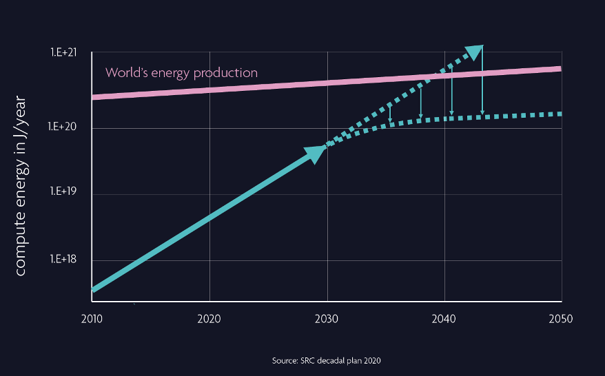
During imec’s satellite event on Monday of SEMICON WEST week, Luc Van den hove, President and CEO of IMEC, kicked off the evening with a summary presentation of programs pertinent to the semiconductor industry that IMEC is coordinating. The research institute recently launched a sustainability program that is initially focused on reducing the carbon footprint for semiconductor manufacturing. Van den hove used data generated by the Semiconductor Research Corporation (SRC) to show that compute energy is rising at a rapid rate and in two decades will approach the level of the world’s energy production (Figure 1).
Van den hove then went on to lay out the scope of IMEC’s sustainability program, which will look at a product or electronic device through its entire lifetime and calculate the carbon footprint and the waste generated (Figure 2).
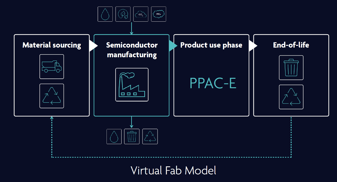
This data will be collected to a certain extent similar to a digital twin, and then let companies see where they can impact their carbon and waste footprint.
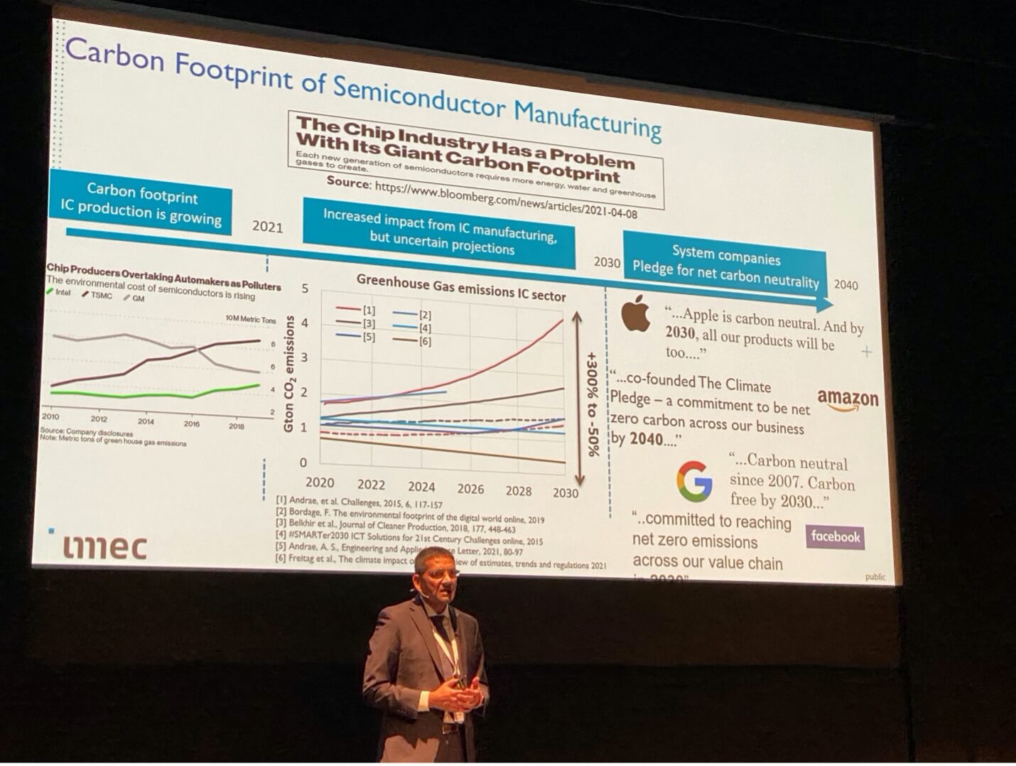
Sri Samavedam, senior vice president of CMOS technologies at imec followed up by giving more details on the program. He presented data from the aforementioned Bloomberg article (Figure 3). Van den hove and Samavedam used this data to highlight the sustainability program IMEC has embarked upon to accurately map the energy used in the semiconductor industry in the operation of the fabs and the different processes. The program is mapping the CO2 energy footprint, as well as the greenhouse gases used in the processes. Apple is the first major industry partner for this program and it will be interesting to see if other industry leaders using semiconductors will join the program.
Samavendam highlighted the fact that with the industry growing at a rapid pace, it is important to look for ways to reduce the energy consumption of both the chip processing but also the compute energy that is increasing rapidly as edge compute and artificial intelligence (AI) roll out.
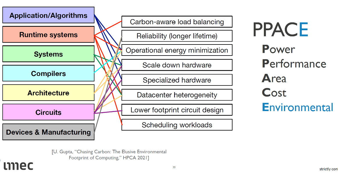
Jan Raby, CTO at IMEC and Professor at UC Berkley, presented A Future Shaped by Energy, in which Raby discussed the future elements of compute and proposed some avenues to reduce the energy used in the compute functions of the future. All three presenters highlighted that in addition to power performance area and cost (PPAC), the industry needs to include an E at the end or possibly a G (PPAC-E or PPAC-G) to help keep the industry aware of the need to reduce the carbon footprint, as well as reducing waste (Figure 4).
Innovation to Reduce the Carbon Footprint
While IMEC kicked off the show from a sustainability perspective, SEMI ended the show on a sustainability note, with an update on the Semi Sustainability Initiative. Much of the information here was presented back in October at the SEMI Sustainable Venture Forum.
The presentations were essentially an update of the need for an industry-wide sustainability effort, with Mary Majors of EMD reviewing the chemical side of the equation, and reminding us that gas and chemicals also play a role in greenhouse gasses (GHG). This was followed by Fawn Bergan discussing the efforts at Intel.

What I probably appreciated most about this session was the S&P Global presentation by Grace Kao who gave an excellent breakdown on Scope 1, 2, and 3 emissions, as well as highlighting some of the challenges with the measurement of Scope 3 measurements.
Lars-Ake Ragnarsson, of imec, reviewed the details and findings of the IMEC program. The information is a good start for the industry, but for me, one of the disappointments of imec’s presentation was that conclusion was that Scope 2 emissions were the major source of CO2, and that the key recommendation was to increase the amount of renewable energy for the industry. I was a bit disappointed in the recommendation that there was not a suggestion to look at reducing a fab’s power consumption as well.
To a certain extent, I look at companies just switching to renewables, without also figuring out how to reduce power consumption, as just kicking the emissions problem down the road. With rare earth challenges, conflict metal issues, and a lack of proven recycling capability for the renewable energy components, I can envision an entirely new set of problems that we will face in the next 10 or so years, a bit like the paper or plastic bag challenges we are facing now where we see plastic bags everywhere and they are a significant source of microplastics in the environment.
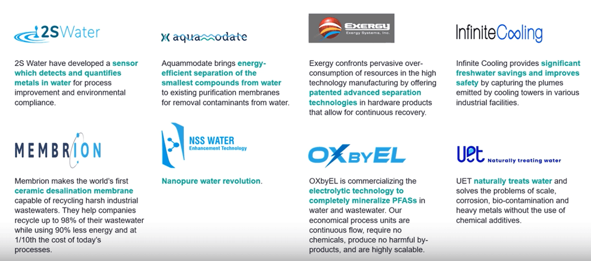
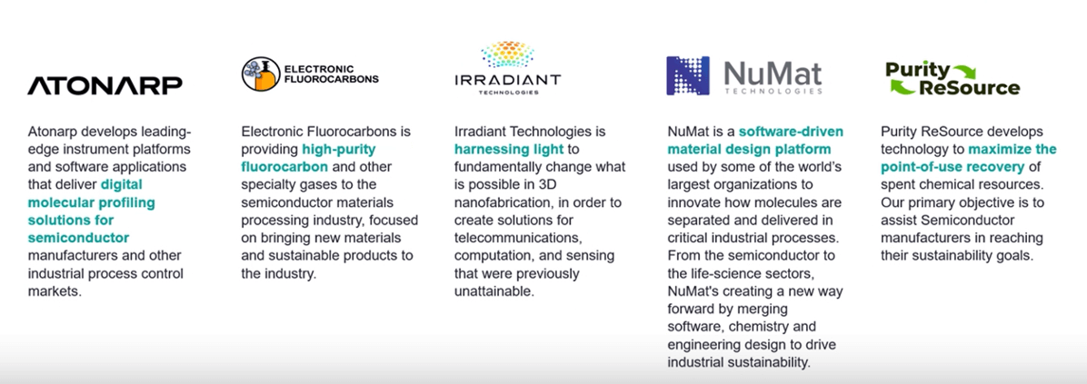
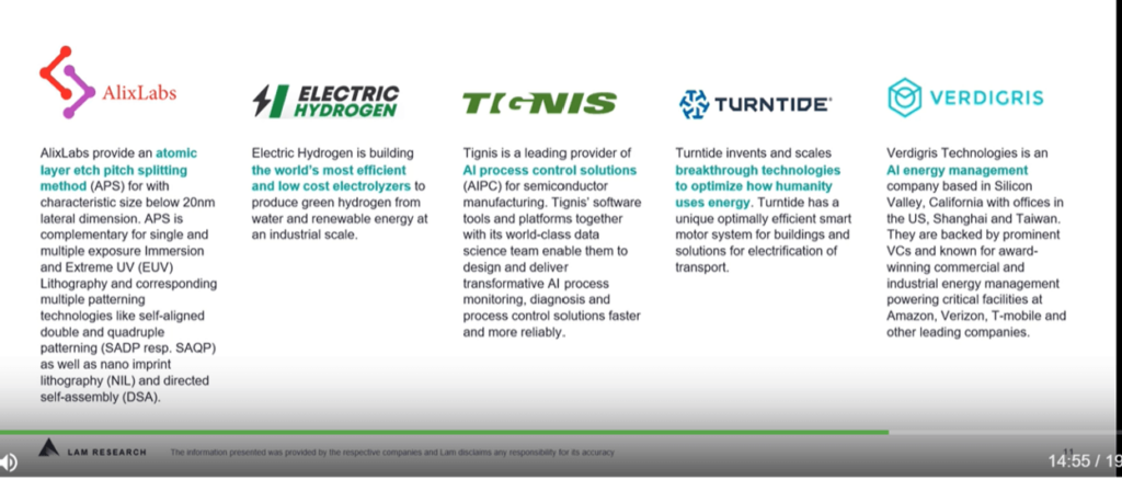
This is why the Semiconductor Sustainability Pitch Event is important for the industry (Figure 5). Whether semiconductors need a new perspective or just new ideas for addressing how semiconductors are structured and manufactured to assist in reducing the industry’s carbon footprint. And what is exciting about this is that a significant part of the semiconductor community is behind this and is supporting these startup companies.
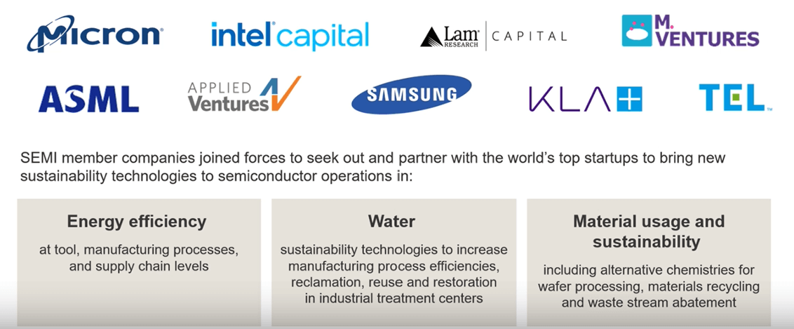
Faran Nouri, Managing Partner, Lam Capital, had the privilege of announcing the semifinalists of the SEMI Sustainability Initiative (Figures 6-8). These are start-up companies that have presented proposals to the VC organizations that were present at the meeting in September. Finalists will be selected in water, energy efficiency, and material usage, and sustainability. SEMI and the VCs had hoped to announce finalists at the show but due to unforeseen circumstances, they will now be announcing the finalists in January.
From a sustainability perspective, this is an exciting time in the semiconductor industry. Most, if not all companies, have published at least one if not multiple editions of their ESG goals. There is a strong focus and VC support on solutions on ESG projects and meeting ESG goals. And the industry is looking at innovative ways at reducing its greenhouse gas footprint. Improving abatement percentages, innovating new chamber clean processes, and cross-collaboration to develop procedures to reduce energy consumption by idling pumps and process chambers when not being utilized. While the semiconductor industry may have a carbon emissions problem. It is reacting quickly to see how to reduce it. It will be fun to see how the startup companies above can impact and reduce the industry’s GHG footprint.


