
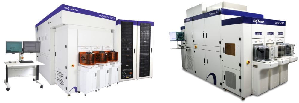
MILPITAS, Calif., July 10, 2018—Today KLA-Tencor Corporation (NASDAQ: KLAC) announced two new defect inspection products, addressing two key challenges in tool and process monitoring during silicon wafer and chip manufacturing at the leading-edge logic and memory nodes. The VoyagerTM 1015 system offers a new capability to inspect patterned wafers, including inspection in the lithography cell immediately after the development of the photoresist when the wafer can be reworked. The Surfscan SP7 system delivers unprecedented defect detection sensitivity on bare wafers, smooth and rough films—essential for manufacturing silicon substrates intended for the 7nm logic and advanced memory device nodes, and equally critical for earliest detection of process issues during chip manufacturing. Together the two new inspection systems are designed to accelerate time-to-market for innovative electronic devices by capturing defect excursions at their source.
“With leading IC technologies, wafer and chip manufacturers have very little room for error,” said Oreste Donzella, Senior Vice President and Chief Marketing Officer at KLA-Tencor. “Critical dimensions of next-generation chips are so small that the minimum size of a yield-killing defect on bare silicon wafers or blanket-film monitor wafers has shrunk below the detection limit of available tool monitoring systems. A second key gap in the defect detection space has been reliably detecting yield-killing defects introduced early in the lithography process, whether 193i or EUV. Our engineering teams have developed two new defect inspection systems—one for unpatterned/monitor wafers and one for patterned wafers—that provide a key capability for engineers to address these difficult defect issues rapidly and accurately.”
The Surfscan SP7 unpatterned wafer defect inspection system achieves its game-changing sensitivity through substantial innovations in illumination and sensor architecture that produce decades of improvement in resolution over that of the previous-generation, market-leading Surfscan tool. This unprecedented leap in resolution is the key to detection of the smallest killer defects. The new resolution realm also enables real-time classification of many defect types, such as particles, scratches, slip lines and stacking faults—without removing the wafer from the Surfscan tool or affecting the system throughput. At the same time, exquisite control over peak power density allows the Surfscan SP7 to inspect thin, delicate EUV photoresist materials.
The Voyager 1015 patterned wafer defect inspection system closes a long-standing industry gap in after-develop inspection (ADI), leveraging novel illumination, collection and sensor architecture. This revolutionary laser scattering inspection system drives sensitivity forward while reducing nuisance signals—and delivers results substantially sooner than the next-best alternatives. Like the new Surfscan SP7, the Voyager system features exceptional control of power density, allowing inline inspection of delicate photoresist materials after develop. High throughput capture of critical defects in the litho cell and other modules of the fab allows process issues to be identified and rectified rapidly.
The first Surfscan SP7 and Voyager 1015 systems have been operating at leading wafer, equipment and chip manufacturers worldwide, where they work together with KLA-Tencor’s eDR electron-beam review systems and Klarity data analytics systems to identify process control issues at the source. To maintain the high performance and productivity demanded by wafer and chip manufacturers, the Voyager and Surfscan SP7 systems are backed by KLA-Tencor’s global comprehensive service network. More information about the two new defect inspection systems can be found on the Voyager 1015-Surfscan SP7 launch information page.
About KLA-Tencor:

KLA-Tencor Corporation, a leading provider of process control and yield management solutions, partners with customers around the world to develop state-of-the-art inspection and metrology technologies. These technologies serve the semiconductor and other related nanoelectronics industries. With a portfolio of industry-standard products and a team of world-class engineers and scientists, the company has created superior solutions for its customers for more than 40 years. Headquartered in Milpitas, Calif., KLA-Tencor has dedicated customer operations and service centers around the world. Additional information may be found at www.kla-tencor.com (KLAC-P).
Forward-Looking Statements:
Statements in this press release other than historical facts, such as statements regarding the expected performance of the Voyager 1015 and Surfscan SP7 systems and the economic effects of defect reduction for wafer, equipment, materials and chip manufacturing facilities, are forward-looking statements, and are subject to the Safe Harbor provisions created by the Private Securities Litigation Reform Act of 1995. These forward-looking statements are based on current information and expectations and involve a number of risks and uncertainties. Actual results may differ materially from those projected in such statements due to various factors, including delays in the adoption of new technologies (whether due to cost or performance issues or otherwise), the introduction of competing products by other companies or unanticipated technological challenges or limitations that affect the implementation, performance or use of KLA-Tencor’s products.
