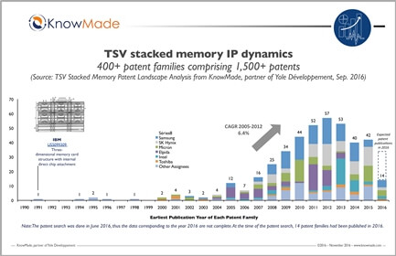
The last two years have shown some important changes within the 3D through silicon via (TSV) memory market. First commercial products including 3D stacked (3DS), DDR4, high bandwidth memory (HBM) and hybrid memory cube (HMC) have been released by the microelectronics giants. Then first 3D TSV IP patent litigations took place between ELM 3DS and leaders such as Samsung Electronics, SK Hynix, and Micron Technology. Indeed, since the mid-2000s, more than 400 patent families relating to TSV stacked memory technology have been published according to TSV Stacked Memory Patent Landscape Analysis (Sept. 2016) from KnowMade, a technology intelligence and IP strategy consulting company.
In the semiconductor industry, 3D integration using TSV has been considered to be a promising way for improving performance and density. Indeed, by connecting stacked chips with the TSV vertical connections, the wide bandwidth I/O and reduction of interconnects length can be achieved.
The 3D TSV market for memory applications is showing an impressive compound annual growth rate (CAGR) to 2020: analysts from Yole Développement(Yole) announce 43% growth with almost 200 thousand units of wafers in 2016.[1]
New products released by the leaders of the microelectronic industry including AMD, Samsung Electronics and more demonstrated the added-value of this innovative advanced packaging platform. The reverse engineering and costing company System Plus Consulting is daily working on these 3D memory devices to explore the TSV stacked technologies and describe the manufacturing process flow.
By combining their technical expertise and their industrial knowledge, the three companies, Yole Développement, KnowMade and System Plus Consulting, namely Yole Group, invite you to discover the status of 3D TSV technologies for memory applications. 3D TSV technology is becoming a key solution platform for heterogeneous integration.
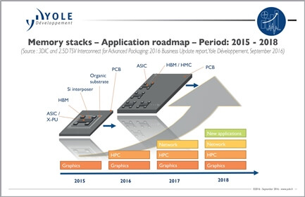
The market for 3D TSV technology will continue to grow, with a CAGR exceeding 10% over the next five years, helped by the next wave of adoptions, especially with 3D memory devices for high-end graphics, high-performance computing, networking and data centers applications.
For example, an HBM has been introduced by AMD in its Radeon™ R9 Fury X high-end graphics card. System Plus Consulting released last year a detailed reverse engineering and costing analysis of this component, titled AMD World’s First HBM-Powered Product SK Hynix 3D TSV High-Bandwidth Memory, highlighting 3D TSV technology added-value in this new component: “AMD’s 3D & 2.5D component integrates HBM such as DRAM dies & logic dies connected with via-middle 3D TSV and micro-bumps as well as GPU stacked onto a silicon interposer including also via-middle 3D TSV,” explains Romain Fraux, CTO’s System Plus Consulting. According to AMD, this HBM component delivers 60% more memory bandwidth, 3 x the performance per watt and consumes 94% less PCB area than GDDR5.
Moreover, both AMD and Nvidia have also announced new graphics products exploiting next generation HBM2 technology.
Other announcements include networking original equipment manufacturers (OEMs) such as Cisco and Juniper Networks with switches and routers integrated with HMC and HBM technology. And memory suppliers SK Hynix, Samsung, and Micron have already announced the specification for third generation HBM3 and HMC3.
Another important market is 3DS DDR4, for servers. Yole’s analysts believe that the market share of 3DS could surpass other 3D memories in next 10 years. Samsung and SK Hynix are already in high-volume manufacturing with 3DS products and Micron too will soon enter this market.
“The TSV stacked memory intellectual property (IP) landscape is today close to the market”, announces KnowMade’s analyst, Dr. Audrey Bastard. “Indeed the 3DS TSV memory IP ecosystem is mainly led by microelectronic giants with some academic applicants and small companies.”
USA and Korea, principally represented by leading microelectronic companies such as Samsung, SK Hynix, Micron/Elpida and Intel, represent the main countries of patent filings. In parallel, the European area seems to show only few interest for patent applicants.
First patents involving TSV stacked memories were already published in the 1990s, but the development of the technology really started in the mid-2000s with a significant increase of patent publications. Today KnowMade observed a decrease of patent applications the last two years, while the first products appeared on the market.
The 5 major players Samsung, Toshiba, Micron/Elpida, SK Hynix and Intel have been profiled by KnowMade’s team. For example, SK Hynix does not present any worldwide IP strategy in 3D TSV memory. Its patents are mainly focused on die memory stacking and interconnections. For several years, the company is developing different approaches dedicated to heat dissipation, adhesion, error failure and more… in the memory stack.
These results will be part of Yole Group’s presentation taking place at Electronics Packaging Technology Conference (EPTC) from November 30 to 03 December 2016 in Singapore.
The Group is also a partner of the European 3D Summit powered by SEMI (Jan. 23-25, Grenoble, France). “The 3D integration of heterogeneous systems aiming at creating more performant and innovative systems keeping a good control of cost is definitely a hot topic,” asserts Anne-Marie Dutron, Senior Director, Business Development at SEMI Europe. “Attending the European 3D Summit will allow professionals to stay up-to-date with all the latest breakthroughs but also with the market changes. A large set of international speakers and keynotes will provide solid assets to the attendees to understand the technologies and market trends.” Yole is playing a key role in the European advanced packaging ecosystem. And its commitment is highlighted by its strong participation within European 3D Summit program.
For more information about Yole Group’s activities within the advanced packaging area, please contact Camille Veyrier or go to i-micronews.com advanced packaging report section.
[1] Source:3DIC & 2.5D TSV Interconnect for Advanced Packaging : 2016 Business Update report, Yole Développement, September 2016
Source: www.knowmade.com


