
While everyone’s waiting for the big memory houses like Micron and Samsung, and IDMS and foundries like IBM and TSMC to announce they are ramping to high volume manufacturing (HVM) with 3D ICs, deep in the heart of Texas, it’s already happening in low volumes for custom applications thanks to Tezzaron Semiconductor and its recent acquisition, Novati Technologies (formerly SVTC Technologies). After the Oct 22 announcement of the completion of the acquisition, I caught up with Bob Patti, CTO Tezzaron and Tim Scott, Director of Business Development of Novati, to find out how all this came about and what the companies’ plans are going forward.
A White Knight Aquisition
As it happened, explains Patti, Tezzaron was looking to bring production to the US, just not quite this soon, or of this scale. He says the company envisioned a smaller fab operation, and eventually planned to move Singapore operations on shore because customers are calling for it. But when it was revealed that SVTC Technologies, which provides semiconductor manufacturing services for such markets as semiconductor, life sciences, aerospace, defense, consumer-mobility and solar energy, was closing its operations in Austin, Texas and laying off 105 employees, an “irresistible opportunity” presented itself.
“Not in my wildest dreams would I have thought of getting the capacity or capability we got by acquiring the Texas fab. It would have been unthinkable if there wasn’t an incredibly short time frame. We were the only ones who could move fast enough to acquire it,” notes Patti, adding that Tezzaron was already doing business with SVTC and had moved all its backside metallization into the facility. “It’s a fantastic opportunity, and gives us a lot more breadth and capability.” He said. Patti also clarified that Tezzaron did not buy SVTC outright; it was an asset purchase which included customers. They hired back all the employees that SVTC Texas had laid off, and as such normal operations were maintained throughout the transition. Novati Technologies is now a wholly-owned subsidiary of Tezzaron.
What’s in a Name?
As it was an asset acquisition, the company name “SVTC Technologies” was not part of the deal. So they held a contest internally for employees to come up with the new name. Apparently it got quite literal. With a goal of being a “center of innovation” the winner used the dead-center letters of “innovation” to come up with “novati”.
But aside from the name change, its pretty much business as usual for Novati. Scott explained that overhead was the problem with SVTC, because they were running two fabs at once. The Austin operation had always been profitable, but the addition of the San Jose facility was a drain. He says running the same business model with one fab and half the overhead cost, while better utilizing the capacity of the fab is what needed to happen earlier. “We’re happy that we’re able to continue with the same business model. We think the Tezzaron relationship is good and there is synergy with what we’re doing,” notes Scott. “If anyone was going to buy us, it was a best option. We think it’s a great relationship, and excited to see what happens in 2013.”
Moving Forward
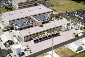 For Tezzaron’s part, Patti says the plans moving forward are to bring the company’s entire domestic manufacturing into the Texas fab and close the fab in Singapore. Tezzaron’s 2.5D and 3D production alone will take up a third of the capacity. “What we would like to see is to bring up more baseline production in the fab,” noted Patti. “Because better consistency benefits all the customers.” With only a third of the capacity taken up by Tezzaron, there’s lots of room to take on additional customers. Additionally, Tezzaron plans to fill up another third over the next year, while also growing Novati’s existing business. “It’s a 92 acre site. There’s lots of land. We can build,” says Patti.
Scott added that Novati would continue serving the customers and business that already exists at the facility. He said the fab handles lots of specialized processing such as MEMS, microfluidics for life sciences, DNA sequencing, photonics, “more than Moore”, and other novel technologies on top of silicon.
3D – “We’re doing this!”
At Novati, Tezzaron has the capability for both front and back-end metallization processes at 200mm, says Patti. At 300mm, the plan is to build entire CMOS process wafers, build devices, and do backside metallization and 3D assembly. Comparing its model for 3D to that of TSMC, Patti says, the company is staging its 3D business as a one-stop-shop for 2.5D and 3D manufacturing. However, unlike TSMC, they work on an open platform model. The company is part of the IME consortium and works to transfer the technology from lab to fab. Ticking off Tezzaron’s capabilities, Patti says the company provides interposer support as well as 3D assembly using silicon produced in-house or other via other sources. Additionally he says they can add TSVs to customer devices or stack memories on their logic devices. He estimates volumes of 3-4 thousand wafers per month and adds, “Today we would cover any volume requirements we’re seeing for the next 2-3 years.”

Patti says there’s been a tremendous uptick in business. “Tezzaron’s business is up more than 500% this year over last, and we’re expecting another 2-300% apart from Novati,” said Patti.
Scott says that Novati is growing also, and that the business model is hitting stride. While the two companies had joint customers before the acquisition, having the fab capability to do 3D manufacturing is precipitating new business. “We’re hoping we can feed off of each other,” says Scott. “Tezzaron open a door for Novati for customers and vice versa. We’re working intimately together in the work that we do. I think we have an excellent opportunity to bring a lot of value to the customers.”
New capability and new equipment from Tezzaron will allow Novati to do more. Scott explained that they do a lot of custom processing, and “esoteric things”. The companies both target government projects from the DoD and DARPA. Patti says while it varies widely from year to year, this year 85% of Tezzaron’s business is DoD and government. Scott says the companies are working towards the distinction of “government trusted manufacturing” from design through to package and test through the Trusted Foundry Program. Scott explained that to be ‘government trusted” the company must be US owned, manufacture on-shore and use domestic sources of supply. IBM was the first “trusted” foundry. “The government is looking to have trusted sources so they have some assurance that no one is likely to stick in ‘funny circuitry,” explained Scott.
It’s really no surprise to me that Tezzaron is once again pioneering a path for 3D ICs. Sure it’s not a commercial application or being manufactured in high volume. But they’ve taken the technology way beyond prototypes and test chips.They’ve found customers who put performance before cost. In my book, that qualifies as doing it. ~ F.v.T.


