
Accomplishment
Licensees of Adeia’s DBI Ultra hybrid bonding process include but not limited to Micron, SK Hynix and Samsung .
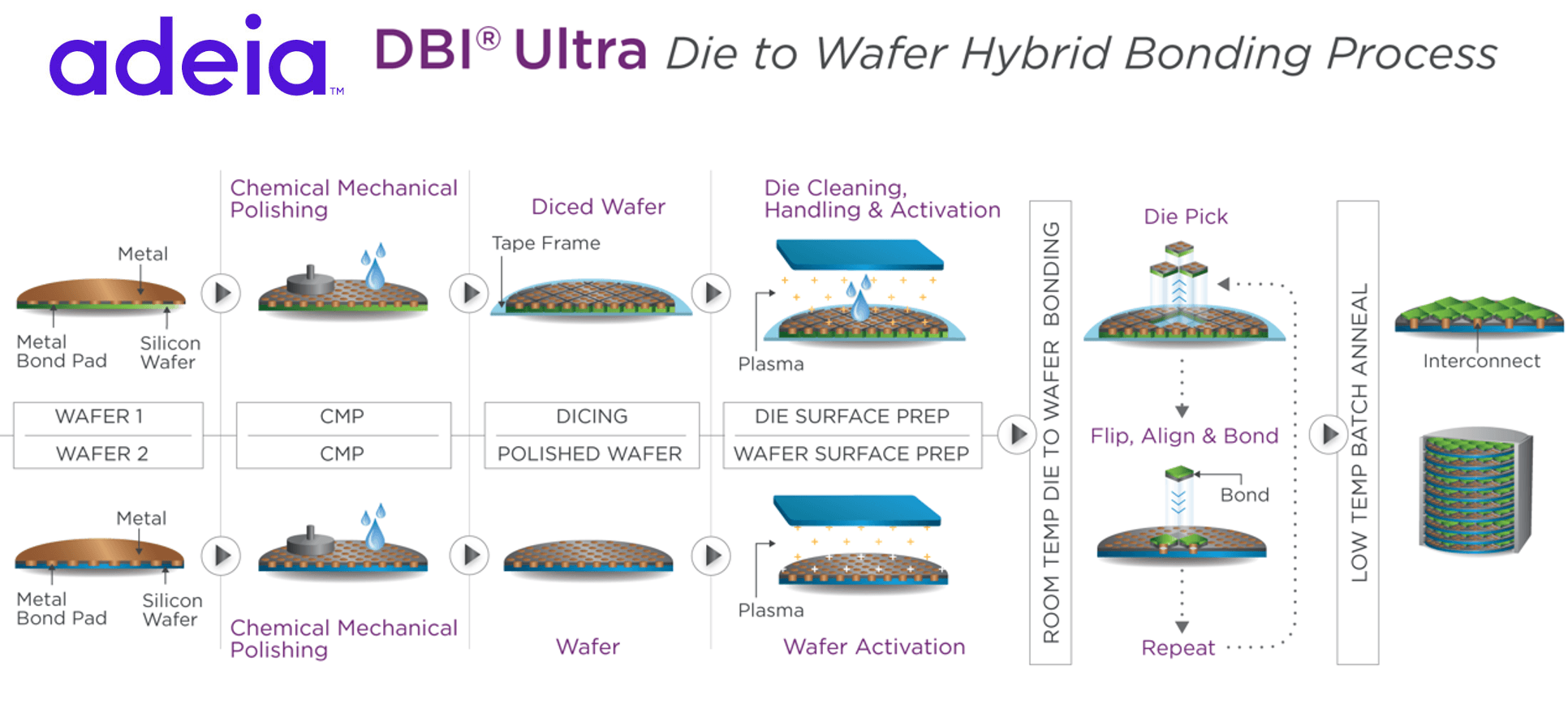
DBI Ultra enables low-temperature die-to-wafer (D2W) or die-to-die (D2D) hybrid bonding at very fine pitch and is licensed by major semiconductor companies around the world. Besides 3D memory stacking, it is getting increasingly popular in high performance logic (CPU, GPU, SoC, etc.) and is expected to be used in various types of heterogeneous integration.
Adeia pioneered this game-changing, beyond Moore’s Law 3D integration technology to enable greater functionality, higher bandwidth and smaller size for next generation semiconductor devices. DBI Ultra accommodates stacking of dies of different sizes, on wafers from different technology nodes, different substrate/wafer materials, providing unprecedented flexibility in 2.5D and 3D integration and large die disaggregation with 3D chiplets.
To learn more about DBI Ultra, please visit https://adeia.com/dbi-die