Accomplishment
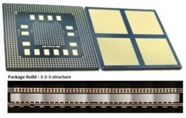
The continuing trend towards miniaturization, system cost reduction and shorter time to market for electronic products drives the need for heterogeneous integration of larger number of components in a single module. AT&S is focused on providing highly integrated and efficient interconnect solutions leveraging large Panel based technologies (PCB, SLP, IC Substrate) for Component Integration (Embedded Component Packaging ECP® ), Ultra fine line Structuring Technologies (SAP) and high speed materials. In the last years, customized solutions for multiple die integration using high accuracy assembly tools (+/3µm) as well as solutions for high density fan-out (L/S ≤5/5um, Via ≤30um) that deliver improved performance, miniaturization and differentiation have been demonstrated by AT&S. Moreover, the existing high-volume manufacturing PCB and IC substrate infrastructure can be leveraged to a large extent which offers attractive potential for volume scaling.


