


Accomplishment
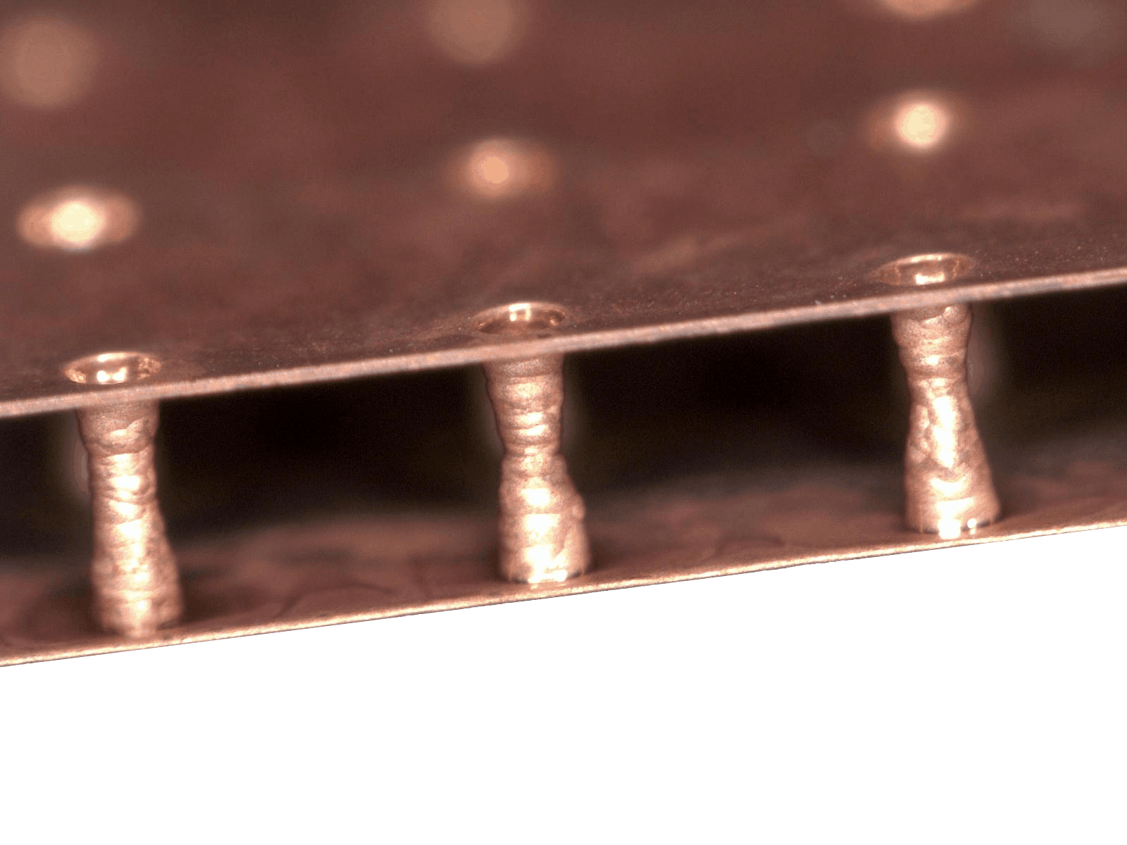
The progressive miniaturization, increasing integration density and requirements for more powerful signal routing create the need for 3D integration. Interposer technologies for rewiring have been developed for efficient communication with high transmission rates in the 3D chip stack or 3D system package. But: There is no established solution to produce glass interposers at wafer level, which provides all required properties for high-frequency applications. For this reason, Plan Optik has developed a new process to apply copper layer on glass wafers, which is particularly suited for high-frequency applications, like for example 5G broadband transmission, radar and imaging sensors, biosensors or beam steering networks. This process will be used for Plan Optik’s Cu-Interposer which can be produced as a wafers, panels or boards. Further products, manufactured with the mentioned process - like Glass-Circuit-Boards with IPD's - will come soon.