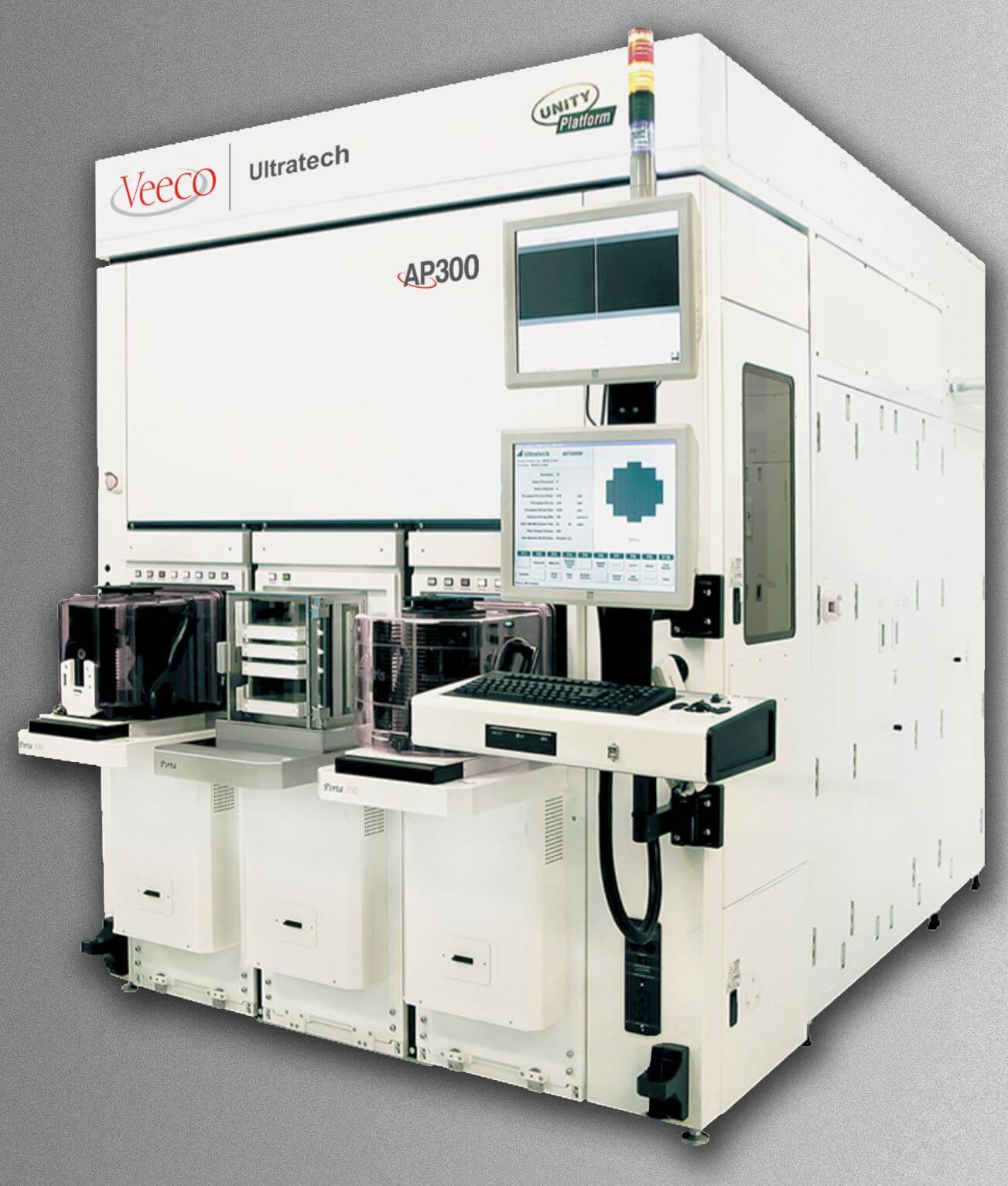
Accomplishment
Launched in 2004, AP300 lithography system’s overlay, resolution and broadband exposure flexibility has consistently driven highly automated, cost-effective manufacturing valued by foundries/OSATs for fan-in WLP, FOWLP, TSV, silicon interposer and Cu pillar bumping. The stepper’s variable NA lens can be optimized to maximize DoF while maintaining higher-resolution performance. Its pattern recognition approach eliminates the need to re-tool reticles for custom alignment targets. It can process wafers with up to 7mm of warpage and the configurable optical system provides a full-wafer topography map for optimizing the focus position for each exposure. The system’s modular architecture helps meet a fabs’ specific requirements and is designed for easy extendibility to accommodate future process nodes. In 2018, the world’s largest OSATs and leading memory chip manufacturers purchased multiple AP300 systems, citing its superior uptime, lower CoO and exceptional performance as key factors.


