
It’s been many years since I realized that semiconductor conferences were not purely scientific but had a certain mix of marketing razzmatazz. Well, the 3D NAND razzmatazz was in full swing last week at the 2015 Flash Memory Summit in Santa Clara, California.
I went along for two reasons. The first was to attend “Creating the Foundation of Flash – A Conversation with Eli Harari” and the second was to gauge where the industry is with 3D NAND.
The first was a marvelous mix of history, science, creativity, teamwork and the magical entrepreneurial essence of Silicon Valley.
The second I’ll try to summarize here.
The Summit took place at the Santa Clara Convention Center between August 11th and 13th. It was a sight to behold with thousands of participants milling around. All the great and good of the Flash memory industry seemed to be present.
The importance of 3D NAND was emphasized in keynote presentations from all the major manufacturers. The language was of the attractive, optimistic, razzmatazz variety:
- “Realizing the Future: 3D NAND” – Micron
- “3D NAND Flash: Tall is the New Small” – Sandisk
- “…. will mushroom in importance” – Samsung.
The Toshiba keynote speaker showed a foot-high 3D printed model of a section of their new 48 layer stack.
Samsung, Toshiba and Sandisk had all previously announced the introduction of 256 Gbit 48 layers and 3 bits per cell.
The exhibits hall too was festooned with impressive models with flashy lights and helpful video displays telling us why 3D NAND is so exciting and important.
Don’t get me wrong. I didn’t really expect much technical detail from a stroll through the exhibits hall. In fact I did learn that SK Hynix seems to be pursuing a U-shaped pipe-based 3D NAND similar to Toshiba’s p-BiCS approach. At least that’s what the impressive video display showed.
None of the exhibit stand representatives could answer my basic questions:
- How many layers can you get to?
- Can you get to 96 layers?
- Are you shrinking the lateral dimensions?
- When does TLC expire as a function of string length (height)?
Mind you, I probably wouldn’t answer these questions either if I were them. These go to the fundamental challenges of their 3D NAND structures.

The possibility, of course, is that even their company experts don’t know the answers. So much is riding on the success of 3D NAND that fundamental challenges may be viewed as optimizable engineering problems by those whose technology and product roadmaps depend on it. For them, optimism is a moral imperative.
A couple of more objective presentations caught my eye:
- 3D NAND Technology: Implications for Enterprise Storage Applications by H. Yoon at IBM
- Comparison of 20nm & 10nm-class 2D Planar NAND and 3D V-NAND Architecture by Choe at TechInsights.
IBM’s presentation explains what the 3D NAND challenges are and what is possible if they are overcome. TechInsights’ presentation is a nice feast of physical analyses with the conclusion that 48 and 64 layers would be possible but not 96 and 128.
What do I make of all of this? First a couple of points:
- The first is to understand that all the manufacturers need to show that there is a smooth roadmap to continued bit cost reductions and density increases. The cat is out of the bag on 2D NAND running out of steam and therefore 3D has to be the path.
- The second is that, although it may appear that the NAND manufacturers are in cutthroat competition with each other, they are really all in the same boat and need a collective success which will help grow the total market for their chips.
So, given these, you can understand the 3D NAND razzmatazz and the bright, optimistic language about the future.
Let’s, however, put on the dark glasses and turn down the volume a bit to see what is lurking in the technical shadows.
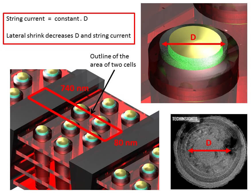
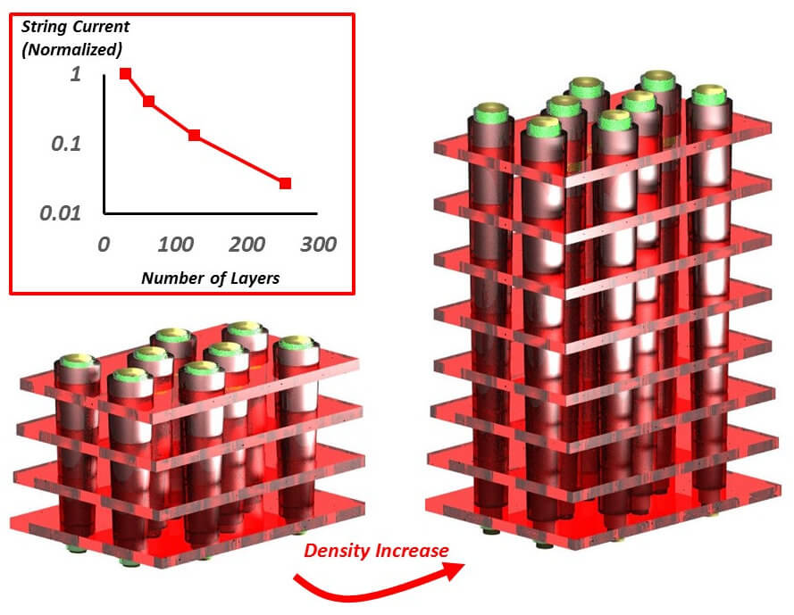
Apart from the manufacturing hurdles, there are extremely interesting device physics challenges that I have discussed before and which are summarized in Figures 1 and 2. Basically, increasing memory density conspires to decrease already small string currents. Approaches to mitigate against this put the ability to do multiple bits per cell in jeopardy. It remains to be seen if this is fundamental or optimizable. I tend towards the former.
All is not doom and gloom however. The industry is full of bright, enthusiastic and optimistic people. The challenge is clear. In that spirit, The feature image on this post is tongue-in-cheek showing one of the glitzy 3D NAND models in among other tall things that mankind has made in the past.
~ A.W.