

Now that we’ve determined that advanced wafer level packaging — including embedded technologies, fan-out wafer level packaging, and 3D packaging — add value to the devices in which they are implemented, the next step is understanding which option offers the best cost/performance ratio for specific product applications. One of the goals of this year’s European 3D Summit was to bring together those who are developing the technologies, and those who are implementing them in there products to figure this out, and to understand where to focus further development.
High performance computing has been the entry point for 3D TSV technologies, as it can bear the cost in exchange for the performance benefits. As this space is an unlikely candidate for FOWLP, researchers are continuing efforts in optimizing fine-pitch 3D technologies. Severine Cheramy, CEA-Leti, and Eric Beyne, imec, each talked about their respective progress. Cheramy focused on Leti’s research institute’s progress in fine-pitch 3D integration, and Beyne focused on scaling for 3D system integration. Both presentations discussed work being done in wafer-to-wafer and chip-to-wafer stacking. Beyne’s focus was on scaling the actual TSVs and bumps, and joints. He also talked about wafer-to-wafer hybrid bonding, and re-visited the concept of system partitioning. (Figure 1).
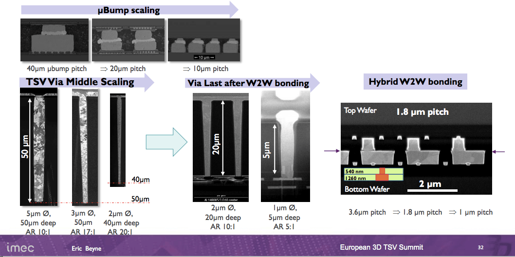
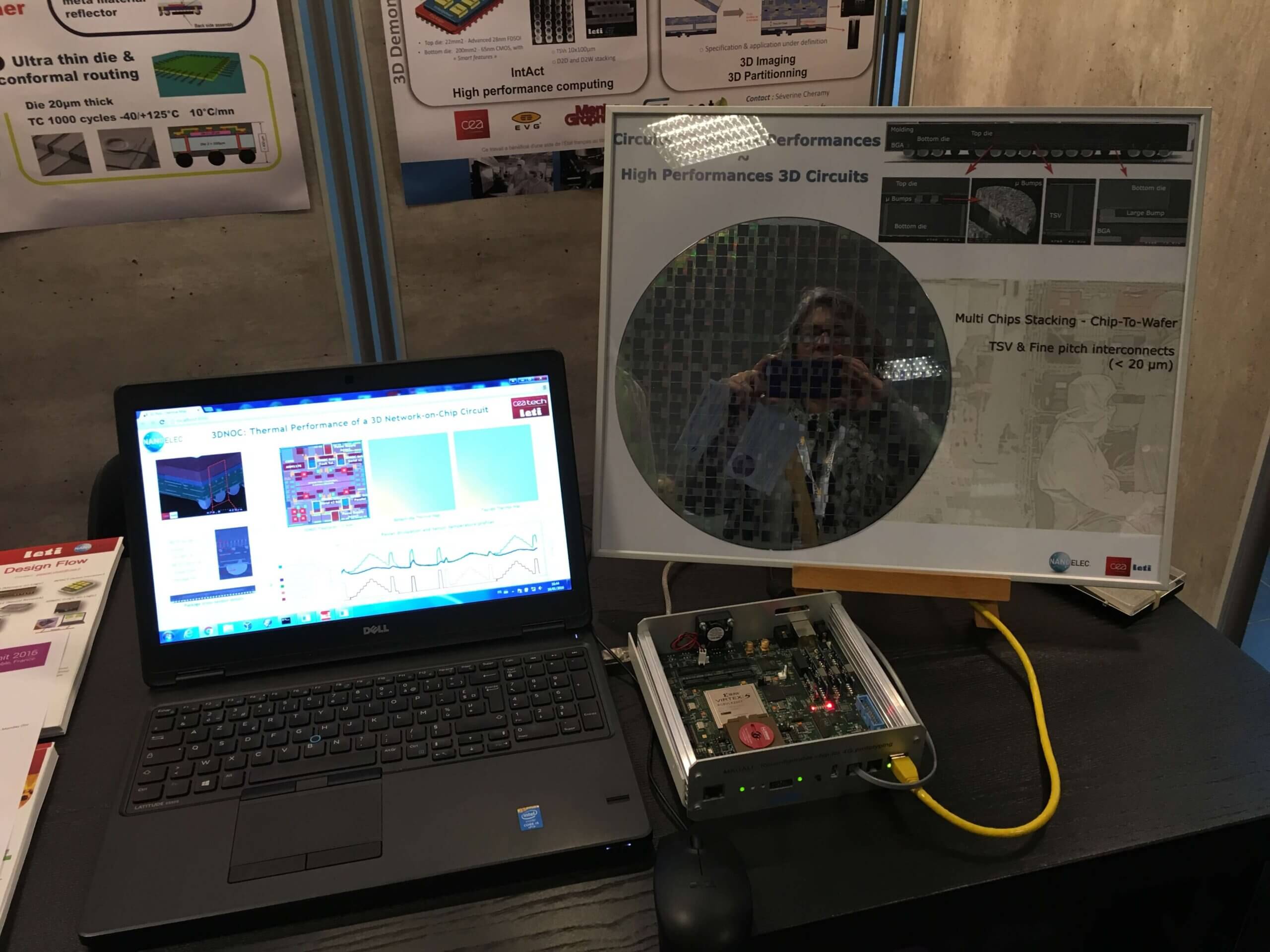
Cheramy stressed that interposer technology is a must for high performance/low power applications. Leti’s solution is to use chiplets on interposers that may or may not have memory integrated. The function of chiplets is performance. Die are partitioned into generic functional blocks that are easy to design and can be re-used application after application. She said the yield for the chiplets will be better in advanced nodes. (This sounds very similar to the work Subu Iyer has launched at UCLA, but he calls them dielets.) In July 2015, Leti introduced the 3D Network on Chip using the chiplet approach during SEMICON West. They had the demonstrator set up at their exhibit at the summit (Figure 2).
Cheramy also provided an update on the IRT NanoElec 3D consortium, which EV Group and SET have recently joined to work on fine-pitch production processes. They are focused on developing highp-accuracy/high-speed chip-to-wafer direct bonding processes using self-assembly. High-aspect ratio vias are another area of focus for Leti. They are working together with SPTS and aveni on an alternative technology for TSV filling to meet aspect ratios >15:1.
There was a lot of representation from the FOWLP space, with market updates from TechSearch and Yole Développement, and presentations on specific technologies by Steffen Kroehnert, Nanium, Dave Hiner, Amkor, and Rama Alapati, GlobalFoundries, who focused on high density fan-out (HDFO). As I recently covered these at previous conferences, let me just summarize by saying that while conventional FOWLP (eWLB) has the potential to replace flip-chip chip-scale packages (FCCSP) and ball grid arrays (BGAs), HDFO challenges interposer-based technologies in performance and signal to noise ratios. The main difference between FOWLP and HDFO is the finer line/space requirements that HDFO can achieve due to different manufacturing processes. For example, eWLB starts with placing die face down on a molded wafer, and then performing the RDL. Amkor’s SWIFT and SLIM starts with the RDL layers on a sacrificial wafer, and then the die are attached and underfilled, followed by mold.
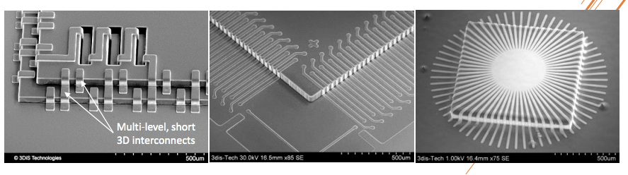
One newcomer to the 3D interconnect family presented at the 3D Summit was a process called 3D RDL, introduced by Ayad Ghannam, 3DIS Technologies, and targeting 3D system integration. Ghannam explained the concept of creating peripheral 3D interconnects using 3 lithography masks. He says this enables “native” 3D system integration without wire bond, TSV or PoP (Figure 3). Target applications for this technology are RF and mm-Wave applications, IoT and multi-chip applications, and MEMS and sensor packaging. Ghannam showed a number of interesting photos and diagrams. It reminded me a bit of the Vertical Circuits technology. The interconnect approach achieves 15/20µm L/S on a 120µm vertical step. As this is bigger than FOWLP’s 10µm l/s already in production, I don’t quite understand the advantages of this, or how to achieve high densities with this approach, but then again, I’m not an engineer. Still, it was interesting to see yet another new idea.
Even the printed circuit board (PCB) manufacturers want a piece of the advanced packaging action. We heard from Heinz Moitzi, AT&S AG, who explained the company’s laminate based embedded component technology (ECB). ECB uses the space in a printed circuit for active and/or passive components, which will be integrated in the core of the PCB core and connected by copper-plated micro vias. ECB is in production, says Moitzi, and it satisfies all the check-boxes: miniaturization, electrical performance, mechanical performance, thermal management, with added benefits of EMV shielding, supports modularization, low set-up costs, and offers and anti-tamper security element. Moitzi said ECP is being used in wearables, modules for wireless connections, medical products, Identification, and fan-out for fine pitch ICs. What I don’t understand is what makes this technology a 3D packaging approach?
The Target Products
Laurent Cargemmel, ATOS, talked about the company’s strategy for implementing 3D in its next-generation Bull Sequana supercomputer. He mentioned Xeon-EP, Xeon Phi, and Nvidia GPUs – Xeon Phi integrates Micron 3D memory stacks. He sees the advantages that the industry has been promoting, such as improved performance, reduced power, improved latency and bandwidth, and lower system cost.

Keynote speaker, Li Li, Cisco Systems, talked about how realizing the Internet of Everything relies on the next-generation of computing, network and storage systems, and that scaling alone is not the answer, as it is too costly. The key to success? You guessed it: 3D memory architectures and 3D packaging. While this is the story we’ve been telling for several years, its exciting to see that the customers are also in agreement.
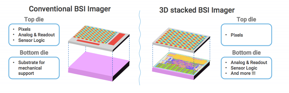
After HPC, we heard from the image sensor sector, where TSVs are king. Jean-Luc Jaffard, Redbelt Consulting, gave a history lesson on image sensor technology, taking us through the evolution from 2D wire bond to 3D stacked backside illuminated (3D BSI) sensors in different varieties that implement TSVs. He said that all variations of BSI will become the standard imaging process. Jerome Chossat, ST Microelectronics, echoed that sentiment, and provided details on ST’s approach for 3D stacked image sensors for smart cameras. His talk focused on the wafer-to-wafer processes using a hybrid bonding approach (Figure 4).
One final presentation centered on products implementing 3D integration was by Martin Schrems, ams. His talk focused primarily on using 3D TSVs for IC sensor integration. He presented a smart system concept using an active interposer, TSVs, WLP and die-to-wafer assembly. Future products implementing these technologies are expected to include environmental and photonics sensors.
Now that 3D ball is finally rolling, it will be fun to watch it pick up steam. On January 19, the second day of the conference, Samsung Electronics announced it has put its second memory product implementing TSVs into production: the industry’s first 4-gigabyte (GB) DRAM package based on the second-generation (HBM2) interface, for use in high performance computing (HPC), advanced graphics and network systems, as well as enterprise servers. It will be interesting what difference a year makes when we gather again for the next European 3D Summit in Grenoble, January 23-25, 2017. Hope to see you there! ~ FvT


