October is a busy month as conferences go. ARM and Intel each held their virtual developer events focusing on the future of compute.
IMAPS addressed packaging technology, and TSMC held its Open Innovation Platform (OIP) forum, also in late October. AMD followed up with an accelerated data center event in early November.
Essentially, in less than 30 days these companies have presented on the future of logic chips and packaging for the foreseeable future. And there is more to come with IEDM in December, and multiple SEMICONs in the near future.
Let’s start with the design and look at the ARM conference first. Simon Segars, CEO ARM, started off his keynote with a walk down memory lane, reminding the audience that the hardware can only be as good as the software that runs it. Segars highlighted the importance of the hardware-software ecosystem ARM has built, announcing that over the past three decades, their customers had shipped over 200 billion chips using ARM technology, 70 billion of those being the low power cortex M.
Segars then introduced the V9 processor, ARM’s new core for their future of computing, that enables developers to create systems from a supercomputer down to a microsensor. Segars touched on that compute, security, and sustainability now all have to be considered when designing a system. Security is still a critical component of the ARM ecosystem; a greater level of security will require changes in how software is written and data is stored.
To help the ARM ecosystem deal with the need for increased security in the hardware and software ARM updated their security manifesto, as well as including confidential compute, an industry-wide security solution, on the V9 core. Security will continue to be a key focus at ARM especially with their involvement with cores for IoT systems, and as their Neoverse server products continue to expand.
Segars also reminded the audience using an example from an ARM client Cloudflare, that ARM’s Neoverse product is helping to decarbonize compute by performing more functions per Watt than was possible with Cloudflare’s previous servers. ARM has announced that they will be carbon neutral by 2023 and will work to assist their clients in decarbonizing compute. With ARM’s broad influence across the ship ecosystem and experience with low power, this will hopefully help the electronics industry lower its carbon footprint, and find ways to reduce the amount of power consumed by compute.
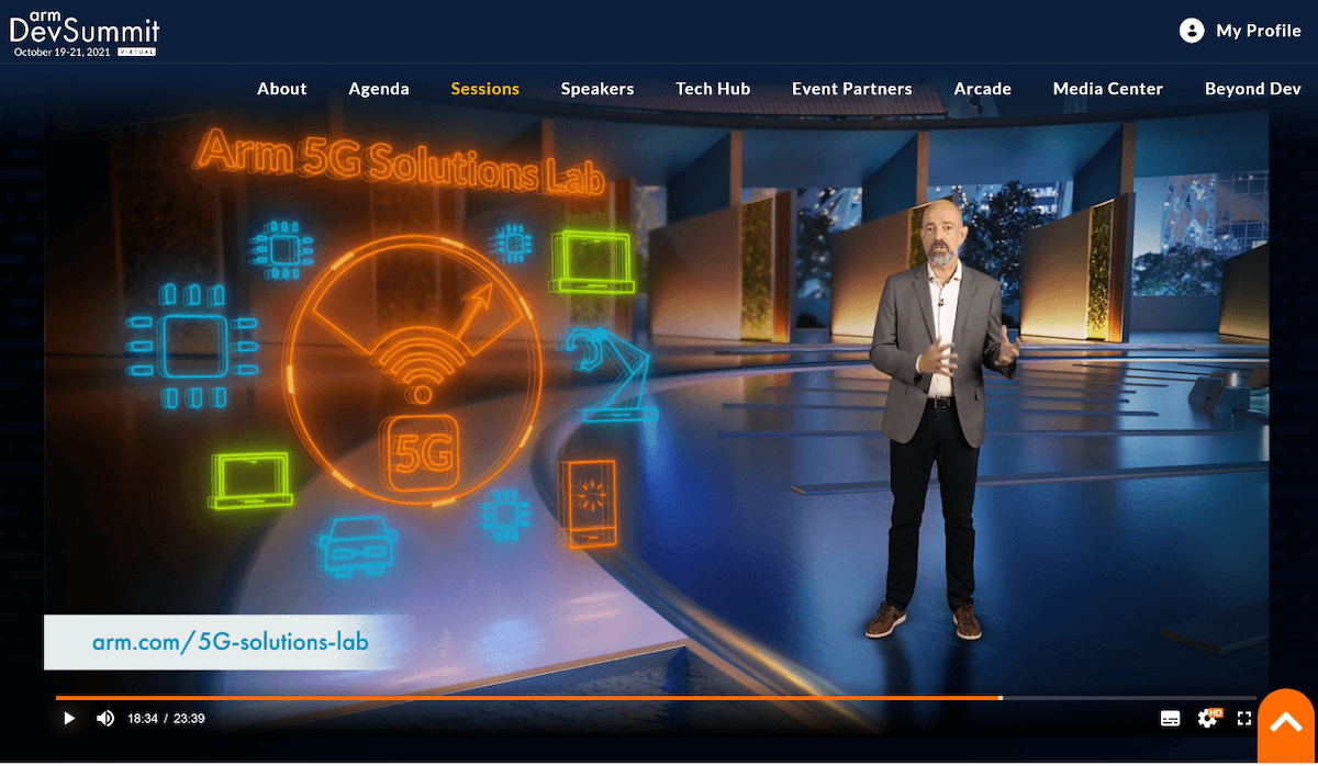
Segars then discussed how ARM is enabling the IoT, with ARM’s total IoT solutions, supporting 5G, with the 5G solutions Lab and working on the development of AI. Segars used the opportunity to promote the pending merger between Nvidia and ARM, as a way to accelerate AI development for the future, where it will be critical to have a successful integration of the software and hardware for both security and low carbon compute.
Cadence 3D-IC platform
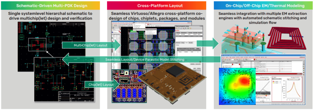
While ARM designs for the heterogeneous compute and embedded systems space, other than helping to facilitate 3D transistors they do little in the 3D packaging space. That is why it was exciting to see Cadence announce its Integrity 3D-IC platform. To date, if your company is working on 3D packaging you are either vertically integrated or most likely working with Intel, or TSMC to get your product to market, and there are limited public EDA tools to help you get your product to market.
The announcement by Cadence now gives companies access to design 3D systems, where before you build you can model and review the entire system chip-to-chip interaction and improve the system’s design to optimize the performance and power before you build.
There are multiple challenges to building 3D packages: Power and thermal challenges, timing challenges, and where to best place different types of chips to achieve optimum performance. The Cadence platform will enable SoC and PCB companies and designers to make the transition to heterogeneous integration and perhaps accelerate or create more options for 3D systems at the packaging houses. It will help with designing significantly as it will help to solidify the standards that have been set for 3D packaging, as well as help with the cadence of tighter pitch on bumping technology The white paper and data sheets suggest that it will speed time to market and make it significantly easier for companies to develop systems based upon chiplet technology (Figure 1).

Intel Innovation Day
After a multi-year hiatus, Intel has brought back its developer conference, now called Innovation Day. CEO, Pat Gelsinger, could also be classified as chief Geek cheerleader, as he was at the center of the 90-minute keynote highlighting Intel’s new direction. While Intel has always been big on hype, it looks like they also have some substance to back up what they are trying to accomplish with respect to regaining the leadership position in the logic transistor race, as well as continuing to drive high performance compute.
During the keynote, Gelsinger discusses the move to what Intel has called the 20A technology node, where Intel will introduce ribbon transistors or gate-all-around (GAA). Gelsinger also discussed monolithic technology or complementary transistors where the transistors will be stacked on top of each other. Some of these technologies will be discussed at length at this year’s IEDM in December, but their introduction to mainstream transistor technology is still a few years away.
In the packaging space, Gelsinger discussed multi-tile, or chiplet technology and Intel’s packaging roadmap, where they are looking at creating an open chiplet ecosystem in their foundry business. This packaging ecosystem would give the chip industry an additional 3D packaging resource that would be located outside of Asia and could help US-based fabless companies in the development of their 3D packaging systems.
The keynote featured a short discussion with Gordon Moore reflecting a bit on Intel’s history, as Gelsinger emphasized that Moore’s law is still alive and well, and Intel expects to be back in the leadership position very soon.
TSMC Open Innovation Platform
TSMC’s annual OIP forum of its foundry platform gives a good snapshot of the status of the industry for TSMC’s customers and partners. TSMC always does a good job of breaking out the business segments and showing the progress and performance of the different sectors they are focusing the business on. TSMC’s roadmap from N5 to N3 has been well documented so there were no real surprises there or in the packaging space. TSMC will present some details from a foundry on the 2.5D/3D integration at IEDM as well as additional roadmap insights.
From a reporter, analyst perspective it’s nice to be able to be briefed in such a short period of time on the future of the industry, and if we missed anything we can catch up with SEMICON, and IEDM, on the near horizon.