
In a recent MEPTEC / iMAPS webinar, Jan Vardaman, President, and Founder of TechSearch International presented growth drivers for advanced packaging and related technology innovations to meet market demand.
Unlike in previous years, when she had to spend part of her MEPTEC presentation explaining what the term “advanced packaging” means and the benefits these technologies offer, during her 2020 Packaging Update there was no need to introduce or sell the importance of advanced packaging, her primary field of expertise.
Major Growth Markets for Advanced Packaging
Computing, graphics, and networking applications demand high performance and high-power packaging, like 2.5D. Mobile devices, like smartphones, smartwatches, medical devices as well as IoT edge nodes drive demand for low cost and lower power multi-die ICs, mostly utilizing wafer/panel-level packaging. DRAMs and Flash memories use vertical die-stacking: 3D-ICs.
Vardaman pointed out that the Covid-19 pandemic is continuing to depress consumer demand for mobile devices, but investments in 5G infrastructure and data centers continue at high levels. (Figure 1)
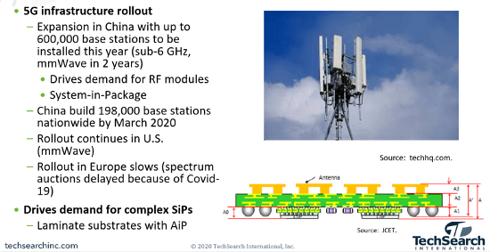
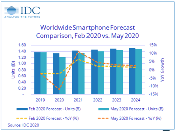
While unit sales of smartphones are likely to decline by 10% year-over-year (YoY) in 2020 (see Figure 2), the increasing complexity of smartphones (e.g. an iPhone 11 Pro Max contains 123 packages from 30 different suppliers) will continue to drive advanced packaging growth. In addition, pent-up demand in 2021 will lead to a projected 10% YoY unit growth. In addition, 5G functionality is further increasing IC content and the number of passives (primarily for filters) in smartphones.
The increasing demand for telemedicine drives the growth of medical devices and smartwatches. Vardaman showed how Ford is encouraging workers with Samsung/Radiant smartwatches to stay at least six feet apart. Over 6000 hospitals and more than one Million physicians are practicing in the USA. No surprise that the American Medical Association (AMA) is asking our industry to develop productivity-enhancing devices for this market.
As a surprise for our industry, the need for social distancing during the current pandemic is driving significant upsides for laptops, tablets, networking equipment, even for more computing power in data centers.
Advanced Packaging Technology Enhancements
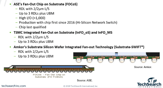
The most important trends in technological advancements are clearly the efforts of package vendors to reduce cost. Wafer/panel-level packaging, replacing silicon interposers with organic substrates and minimizing/eliminating costly TSVs are some of the major developments in progress towards reducing the cost of single and multi-die ICs. As examples, Vardaman showed several fan-out on substrate designs from major vendors (Figure 3).
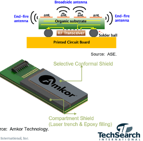
In addition to integrating photonics, Vardaman highlighted that antenna in package (AiP) is a big driver of packaging innovation (Figure 4). Considering that 5G Frequency Range (FR) 1 operates at sub-6 GHz and FR 2 (mm-wave) band operates at about 10x the FR 1 frequencies, antennas are getting smaller and can be integrated, very close to the transceivers, in the package. Important is also that the high FR 2 frequencies demand new materials, to minimize insertion loss (a.k.a. loss tangent) and self-heating.
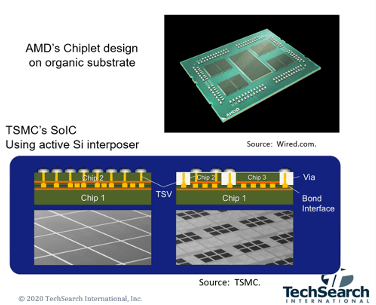
Another important trend in multi-die packaging is the rapidly increasing demand for chiplets (a.k.a. bare dice, known-good dice, hard IP) and for high-speed as well as low-power interconnect technologies for them. Chiplets offer IC and system designers the best of two worlds (Figure 5). Following Moore’s Law, these chiplets can be manufactured at the most suitable (smallest) process node. Also, when integrated in advanced packages, they offer the benefits of More than Moore: designers can combine heterogeneous functions cost-effectively, complement their proprietary chiplet(s) with other (commodity) chiplets in an IC package and reach quickly and efficiently practically any complexity a (sub)system requires. Best of all, this high level of integration improves both performance-per-Watt and form factor by one to two orders of magnitude, compared to individually packaged dice, interconnected on a printed circuit board (PCB).

Vardaman also showed successful examples for multi-die integration, that reduce form factor and extend battery life. Apple’s iPhones and iWatches are leading examples of multi-die integration. Samsung’s smartphones also contain multi-die ICs. Intel’s Lakefield CPU, utilizing the multi-die “Foveros” technology, powers Samsung’s Galaxy Book 5 PC. MediaTek uses TSMC’s InFO oS technology to combine two large logic dice on a substrate. In addition to these recent examples for multi-die ICs, AMD, Broadcom, Nvidia, Qualcomm, Xilinx, and others benefit from their increased performance per Watt and have advanced packaging solutions in production.
Last, but certainly not least, there are other important developments that makes utilizing the above hardware innovations easier and more cost-effective: The major package assembly houses (a.k.a. OSATs) and wafer foundries are developing package assembly design kits (P-ADKs) for their packaging platforms. These P-ADKs guide die and package designers with design rules and constraints on how to optimize performance and reduce development as well as unit cost. Equally important, several of the large electronic design automation (EDA) tools vendors are enhancing the capabilities of their proven die, package, and board design tools to offer user-friendly co-design tools and flows for multi-die integration in advanced packages. Check with your EDA partners, to get up-to-date information about their proven and/or planned die-package-board-system codesign solutions.
Personal Comments
Jan Vardaman founded TechSearch International in 1987. During these 32+ years, she has earned her excellent reputation as the go-to expert on all IC packaging related topics and IC manufacturing in general. Her expertise, the broad range of industry contacts, combined with her commitment to drive and proliferate semiconductor innovations, make her an important contributor to the success of advanced packaging technologies.
Vardaman’s July 15 MEPTEC presentation confirmed that large companies are always the early beneficiaries of new technologies. Much broader market acceptance takes typically several more years.
I am optimistic that three major packaging innovations: availability of 1) P-ADKs, 2) user-friendly EDA tools, and 3) broad portfolio of chiplets will contribute significantly to making multi-die IC design easier, more cost-effective and attractive to many more companies in the near future.


