

Ira Feldman welcomed about 100 attendees to MEPTEC’s December luncheon at SEMI Headquarters to hear Jan Vardaman, Founder and President of TechSearch International deliver her annual “State of the IC Packaging Industry” address titled, “Market Drivers for Advanced Packaging: 2020 and Beyond.”
 In her opening statement, Vardaman emphasized that our industry is significantly exposed to the trade frictions between the USA – where most of the ICs and systems are designed – and China, where a significant number of IC and systems manufacturers are based. Current and longer-term likely consequences for our industry made Vardaman’s 2019 message even more important than in previous years.
Her presentation focused on applications and clearly reflected that our customers no longer build their systems around our semiconductor components. Remember how 20 years ago the “Intel Inside” label was a big selling feature for PCs? Today customers demand our cooperation for solving their system-level challenges.
Major Industry Trends
Vardaman started by describing major industry trends, that will significantly impact our industry in 2020 and beyond:
- PC sales remain slow, amplified by the current CPU shortage.
- Smartphone shipments will slightly increase, driven by 5G adoption.
- Server shipments will increase, especially due to the demand for social media content and data from 5G applications this also benefits AI accelerators used in data centers.
- Another important market for us is automotive. Vehicle unit shipments have declined, but the electronics content in vehicles will increase significantly.
- She also confirmed that IoT edge nodes will become much more intelligent because in situ computing assures privacy and security, reduces response times and total power consumption as well as minimizes traffic jams on the internet.
5G Smartphone Opportunities and Challenges
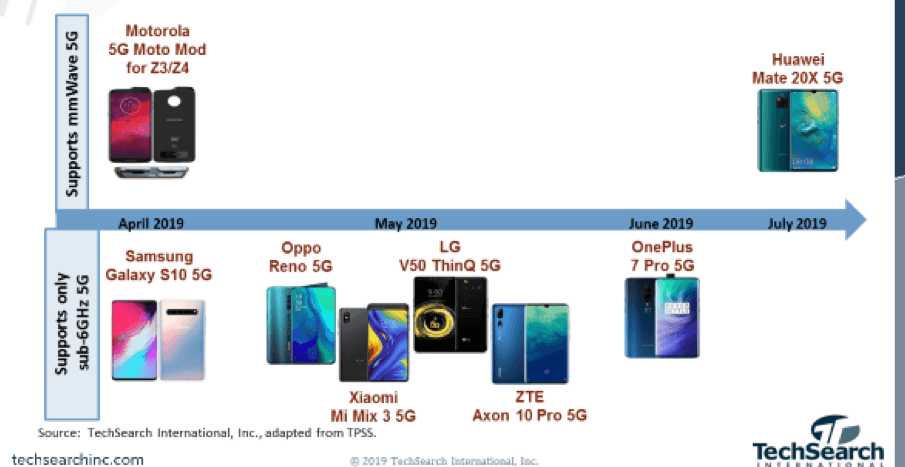
Diving further into the smartphone market, Vardaman outlined both the business as well as the technical aspects. On the business side: IDC projects 1.5% smartphone unit growth, to about 1.5 Billion units shipped in 2020, primarily driven by China sales. Only 14% (=190 Million) will be 5G capable, with most of the units shipped operating at the sub 6 GHz band. The really good news for our industry in 2020 will be that 5G phones need more, larger and more complex advanced packages than the current generation. In addition, to offer good coverage and reliable service, 5G needs several times as many (micro)base stations as we have currently installed for 4G services. This will require major investments by the phone companies (in U.S.: AT&T, Verizon, T-Mobile and Sprint) and limit how fast these companies will be able to build out 5G networks.
On the technical side: 5G phone service will be offered on the “Sub-6 GHz” frequency band (a.k.a. FR 1) and in the “Millimeter Band”, ranging from 28 to 39 GHz (a.k.a. FR 2). While the current 4G and sub-6GHz antennas are centimeters in size and need to be mounted on the PCB, antennas for the ten-times higher frequencies are small enough for integration into packages and modules – a new opportunity for OSATs. Another major 5G challenge (and opportunity for our industry!) will be the many high-quality filters every 5G phone and micro base-station will need. See more about 5G technology basics here.
Because only millimeter wave technology can offer all the promised 5G user benefits and the needed network will take time to cover a large number of customers, only a few 5G-capable smartphones are on the market today. In addition, most of them are “only” sub-6GHz capable ( Figure 2)
Additional challenges with 5G millimeter wave technology
To avoid electromagnetic interference between ICs, conformal (= complete) IC shielding becomes mandatory. However, if one or multiple antennas are integrated into a package, only compartmental (= partial) shielding is possible. Two other points need to be considered:
- High-frequency signals propagate primarily on the surface of a conductor. Surface roughness certainly weakens the signal strength.
- The deployed dielectric materials need to be suitable for the higher frequencies, otherwise what’s called insertion loss will weaken RF signals and the “stolen” energy will heat up the dielectric material (e.g. interposer, substrate, PCB).
A material’s dielectric constant (DK) and dissipation factor (Df) tell if it’s suitable for high-frequency applications. Another important challenge: Millimeter-wave devices and subsystems also demand different test methodologies, compared to 3G and 4G technologies.
Vardaman clearly did not intend to shock the audience with all these new challenges 5G will bring. That’s why she showed how companies address these challenges: Amkor (shielding), ASE (antenna-in-package or AiP), JCET (AiP with build-up and EMI shielding), Various companies including start-ups (filters), IBM Bromont (package assembly and test), Rogers (dielectric materials for 5G) and Teradyne (5G test) have applied their specific knowledge to address and (hopefully) solve all these challenges.
I believe that the industry’s transition to 5G technology is another reason to broaden existing relationships and build new partnerships, to fully leverage existing capacity and your company’s special expertise.

Vardaman did not only cover this broad range of 5G topics. She also addressed recent developments and new requirements for advanced packaging technologies in other major application areas.
Compute servers for data centers
Companies like Alibaba, Amazon, Apple, Facebook, Google, Microsoft, and Tencent manage very large data centers. While their demand slowed in 2019, 2020 is expected to see growth again. The gigantic data volumes IoT edge nodes will provide and the additional compute power needed to fully utilize the power of AI algorithms, to derive value from this data, will further increase the demand for interposer-based multi-die ICs.
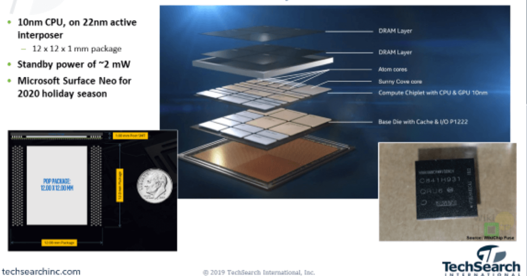
By arranging multiple dice (CPU, GPU, AI-accelerator ASIC, and memory) side-by-side on silicon or organic interposer, improves performance per Watt significantly. Vardaman confirmed that silicon interposers can offer now less than 1-micron line/space pitch and organic materials will allow 2-micron L/S in the future. While TSMC interposers sizes were until recently limited to two times of a reticle field, now TSMC offers interposers up to 2500 mm2 (= three times reticle size). AMD, Huawei, Intel, Nvidia, and others have interposer-based solutions in volume production. Vardaman also emphasized the important role chiplets (a.k.a. dielets or KGD) will play in the near future. As a 3D-IC example, she showed Intel’s Lakefield Hybrid CPU, which uses Intel’s Foveros technology. It combines a 10 nanometer CPU, a 22 nm active interposer and two layers of DRAM. Mircosoft’s Surface Neo, to be introduced in Fall 2020, will rely on this high-performance and low power Hybrid CPU (Figure 3).
Advanced Packaging Challenges in Automotive
As mentioned earlier, most big automotive companies are developing electronic solutions to make their vehicles safer, more secure, more economical and of course more comfortable. Some companies, such as Tesla, are designing their own AI processors for automotive applications. However, legal, cost, and reliability challenges have moved the introduction of the “mobile living room” (a.k.a. Level 5 vehicle) further into the future.
Vardaman focused on the technical challenges that can lead to cracks, resulting in failures. She mentioned that new IC architectures, better materials for underfilling, thermal interface materials (TIM) and packages, as well as lower-temperature manufacturing flows, are needed to meet automotive quality and reliability standards at an acceptable cost. Also, cost-effective sensing technologies, utilizing cameras, radar, lidar, ultrasound, etc. – combined with compute engines and AI algorithms are needed to drive automotive innovation.
Conclusion
Vardaman’s annual “State of the Industry” presentation always gives a great overview of IC packaging technology capabilities and applications. While the packaging technology hardware topics (materials, equipment, manufacturing and test methodologies) are making significant progress towards meeting future requirements, the cooperation between hardware manufacturing experts and electronic design automation (EDA) software suppliers is still limited.
Allow me to add: Both Amkor and ASE are now developing package assembly design kits (PADKs), together with large EDA vendors, because large fabless IC vendors demand that their package design teams deliver accurate and up-to-date inputs, just like the process design kits (PDKs) provide for die-design. I hope that the next TechSearch International Workshop will also discuss materials modeling requirements, simulators for electrical – thermal-mechanical interactions as well as how to expand the current reliability and aging simulators to address multi-physics effects in automotive applications. User-friendly IC package design methodologies will contribute to shorten development cycles, improve performance per Watt, predict failure mechanisms accurately and lower development and unit cost.
I hope that advanced packaging challenges in 5G smartphones, IoT and AI, automotive and Industrial applications will offer enough profits to justify additional software and hardware development efforts for advanced packaging technologies – to win many new opportunities in major markets, as outlined above.
Thanks for reading! Happy Holidays! Success and Health in 2020 and beyond…Herb


