


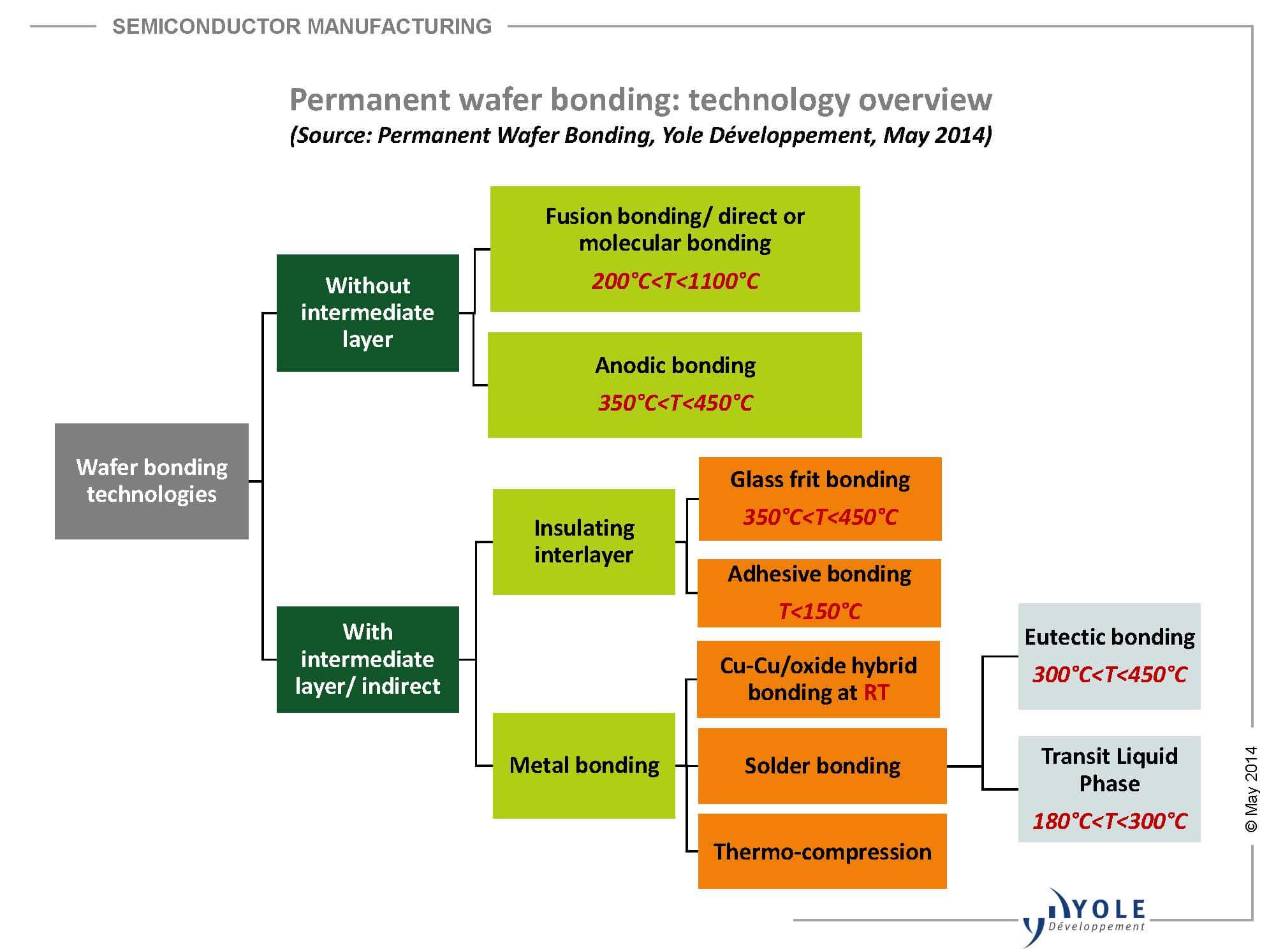
Permanent wafer bonding can be categorized based on bonding with or without an intermediate layer. Intermediate layers can be subcategorized into insulating layers including glass frit bonding, adhesive bonding, or metallic bonding including Cu-Cu/oxide “hybrid” bonding, solder bonding, and thermo-compression copper-copper bonding as shown in Figure 1.
MEMS devices are the main applications using permanent bonding technologies in mass production, followed by CMOS Image Sensor back side imaging (CIS-BSI), LEDs, and SOI processes. The MEMS market is the current main driver followed by CIS-BSI applications. Permanent bonding is well established for MEMs and will continue to grow over the next five years. MEMS bonding is seen moving from glass frit to metal bonding in order to achieve better reliability, better hermeticity, and smaller footprint due to smaller required bond frames.
Adhesive and fusion bonding are currently the dominant technologies used CMOS image sensors. Adhesive bonding is used for near 100% of the attachment of the glass cap wafer to the device wafer. Room temperature (RT) Fusion bonding has become the dominant technology for BSI sensor technology; with anneal temperatures in the range of 20 – 400℃. In the future, Cu-Cu /oxide “hybrid bonding” could become the technology of choice to replace fusion bonding due to its ability to make electrical contact and its superior electrical and mechanical properties. A typical “hybrid bonding” process sequence, developed by Ziptronix, is shown in Figure 2.

Thermo-compression and eutectic bonding are preferred technologies for LEDs grown on GaAs or sapphire substrates.
Fusion bonding is the mainstay for SOI activities. The market has been stagnant due to AMDs recent move from SOI to bulk SI technology which has had significant impact, especially on Soitec. Yole Développement expects the SOI market to double by 2015 due to RF applications making use of SOI.
In 2013, permanent wafer bonding revenue was close to $127M, mostly from fusion bonding and metal bonding technologies. It is expected that this revenue will reach $450M by 2019, growing at a 23% CAGR. In terms of wafer starts, fusion bonding dominates the technology options and will continue to do so out through 2019.

In the next few years, growth is expected from metal bonding for MEMS and Cu-Cu/oxide “hybrid bonding” for CMOS image sensors. Every major CIS player is working on the implementation and qualification of “hybrid bonding” technology for the new generation of BSI CIS.
The Equipment Market
The permanent bonding equipment market is dominated by EV Group (EVG), which holds 75% of market share but is being challenged by the merger of Tokyo Electron and Applied Materials, two of the largest semiconductor equipment suppliers in the world. SUSS MicroTec, which provided permanent bonders for more than a decade, exited the automated permanent bonder market in 2013, but maintained its activities in manual bonders.

About the Authors
This article was co-authored by Amandine Pizzagalli, Technology & Market Analyst, Advanced Packaging and Dr Phil Garrou, Sr Technology & Market Analyst, Advanced Packaging, Yole Développement
 Amandine Pizzagalli is responsible for equipment and materials for Yole Développement’s Advanced Packaging team. She has an Electrical Engineering degree with specialization in semiconductors and nano technologies. She has previous work experience at Air Liquide.
 Dr. Philip Garrou retired from Dow Chemical in 2004 as Global Director of Technology for their Advanced Electronic Materials business unit. Among other undertakings, he is a Sr, analyst for Yole Developpement. He has served as President of IEEE CPMT and IMAPS and has edited several microelectronic texts including McGraw Hill’s “Multichip Module Handbook” and Wiley VCH’s “Handbook of 3D Integration”.


