Examples of Hybrid bonding-related imperfections – misalignment, erosion of dielectric, and over-dishing of copper that can lead to bond failures
Hybrid bonding is emerging for high-performance 2.5D / 3D packaging to improve interconnect performance and density past conventional bump limits.
In this post I’ll give a complete technical overview of the hybrid bonding process flow, key technical challenges, and key equipment makers. This post is based on technical material from several packaging and hybrid bonding experts at IMAPS and ECTC 2026 I personally attended.
A Brief History of Hybrid Bonding
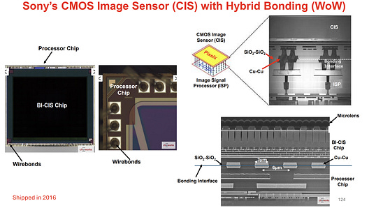
Source: Lau. J. (Unimicron) “Advanced Packaging for Chiplets, Heterogeneous Integration, and Co-packaging Optics” ECTC 2026
Cu-Cu Hybrid bonding is an old form of bonding that was invented between 2004-2005 when ZiBond, a direct oxide-to-oxide bond, was combined with embedded metal bonds.
In 2015, Tessera Technologies acquired Ziptronix for $39 million, adding Ziptronix’s ZiBond and DBI technologies and associated IP portfolio to its advanced-packaging business. Hybrid bonding has been in high-volume production since 2015 with Sony’s CMOS image sensor.
In 2016, Tessera acquired DTS and the parent company renamed itself as Xperi. Xperi merged with TiVo in 2020 and separated into two publicly traded companies in 2022: Xperi Inc, containing the product business, and Adeia Inc., containing the IP-licensing business.
Today, Adeia owns and licenses a substantial semiconductor IP portfolio from Tessera, Invensas, and Ziptronix. In 2025, Adeia initiated a patent infringement suit against AMD’s 3D V-Cache processors. In March 2026 this suit was dismissed with an out-of-court settlement where AMD entered a multi-year license agreement covering Adeia’s semiconductor IP portfolio with undisclosed financial terms.
Classifications of Bonds
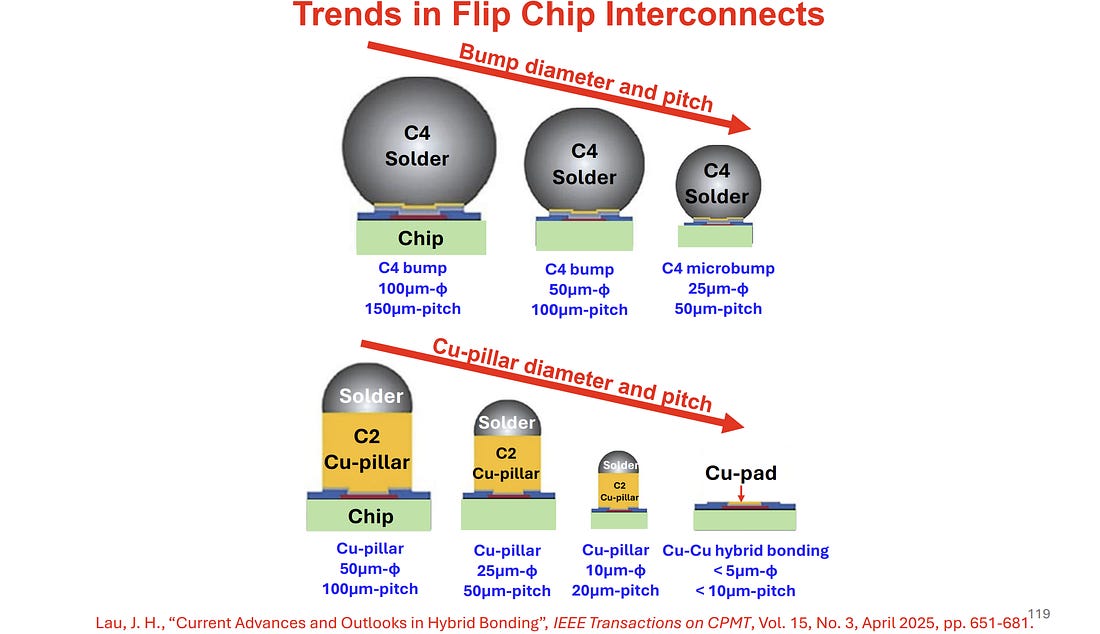
Hybrid Bonding is a bonding option among a few established bonding classifications:
Solder-Based Interconnects
C4 and C2 Pillars are the most widespread interconnect technology today. C4 bumps can have as low as 50um pitch, limited by solder bridging. Cu Pillars can get as low as 20um pitch. Both use standard reflow with heat to melt the solder in between two copper pads using solder and solder flux.
Thermocompression bonding
Thermocompression bonding (TCB) applies heat and pressure to form interconnects. TCB commonly uses Cu pillars + solder cap to form the connection, but direct Cu-Cu TCB can be used as well. Processing temperature and requirements depend on the material and bonding conditions.
Hybrid Bonding
Hybrid bonding goes past TCB to perform both direct Cu-Cu and dielectric bonding. The dielectric is either inorganic (SixOy, SixOyNz, SixCyNz) or an organic polymer.
There are three main ways to perform hybrid bonding:
- Die to Die (D2D). D2D bonds two die together. Both dies must be handled individually, limiting overall throughput, making D2D fairly uncommon relative to D2W and W2W.
- Die to Wafer (D2W). D2W picks singulated known-good die and places them on a common wafer. The prepared surface of the die “sticks” to the wafer with a room temp oxide bond. D2W is flexible, but adds additional processing time for the pick and place machine to physically traverse the wafer.
- Wafer to Wafer (W2W) bonds two wafers together at once. W2W is cost efficient since multiple dies are stacked at once and convenient for simple 2-hi stacks such as stacked CMOS imagers and compute-DRAM stacks. However, W2W lowers overall yield since die yield compounds. In addition, both die layouts and interconnect structures must be compatible with each other.
Performance Benefits of Hybrid bonds
Hybrid bonding has several performance benefits, including:
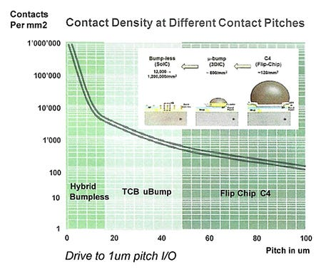
Source: T. Strothmann, “Hybrid Bonding Technology and Markets” TechSearch International.
- More contact density by eliminating solder bridging. Hybrid bonding enables interconnect pitches < 10um and as low as 1um. At ECTC2026, Applied Materials demonstrated 450nm pitch with 98% yield across 20M interconnects, and imec/EV group demonstrated 200nm pitch with < 40nm overlay for 300mm W2W.
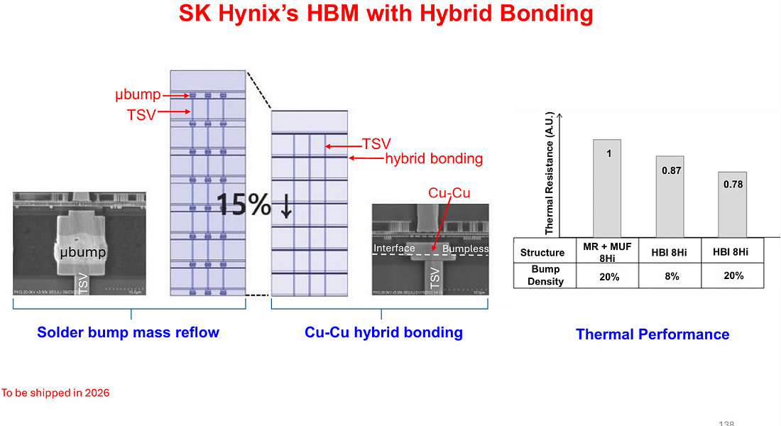
Source: Lau. J. (Unimicron) “Advanced Packaging for Chiplets, Heterogeneous Integration, and Co-packaging Optics” ECTC 2026

- More compact form factor. Hybrid bonding shrinks the vertical interconnect height, enabling shorter die stacks, which is especially important to fit multiple HBM layers in JEDEC package limits.
- Improved heat transfer. Hybrid bonding eliminates the conventional underfill gap from micro bumps and can reduce thermal interface resistance.
- Higher signal bandwidth. Hybrid bonding improves signal integrity due to a lower resistance and impedance discontinuity across the bond interfaces
In summary, hybrid bonding gives more degrees of freedom for system architectures to design chips and systems since it helps mitigate the interconnect constraints that 2D chiplet-based designs bring.
Keep in mind that compared with TCB, hybrid bonding is not the preferred solution for all designs because it comes with a higher cost due to more stringent processing requirements. Hybrid bonding should be used for the interfaces that really need it to push performance, such as 224Gbps+ EIC/PIC-based optical engines, high-density chiplet bridges, and high-layer-count HBM stacks.
Hybrid Bonding Technical Requirements
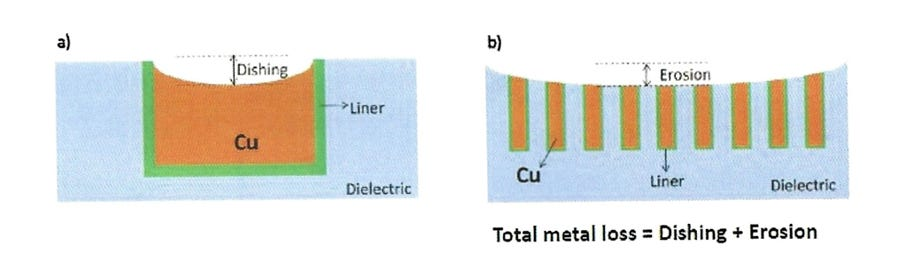
Source: Gottfried, Fraunhofer – IEEE Hybrid Bonding Symposium, Jan, 2026
Hybrid bonding has several stringent requirements:
- Good CMP uniformity. CMP planarizes the entire surface of the wafer/die with chemical reactions and mechanical abrasion. CMP introduces several effects:
- Dishing. Dishing occurs when softer copper is removed from the center of a pad, causing a concave surface. A dishing depth of ~1-10 nm is typical for state-of-the-art CMP, but depends on pad size and specific CMP parameters. A controlled Cu recess is actually desired because it ensures that the copper doesn’t push the oxide apart during expansion. However, both over- and under-dishing can lead to bond failures.
- Dielectric Trenching. Trenching refers to localized recesses in the dielectric adjacent to Cu pads. Trenching is exacerbated by over polishing from CMP, among other factors, and should be minimized.
- Erosion – Erosion is a lower dielectric thickness around dense metal regions. Erosion is dependent on the layout metal density that can affect CMP pressure density. Proper layout techniques are needed to mitigate erosion. Often times, during design, an automated fill routine adds dummy metal shapes to evenly distribute bare metal fill throughout the layout. Large pads also tend to have dielectric openings or arranged into grids to mitigate erosion, dishing, and improve CMP uniformity.
- Flat surface. Warpage is one of the biggest enemies of hybrid bonding. Process parameters such as dielectric material and deposition times can be controlled to minimize die warpage. Warpage is influenced by a few factors:
- Die thickness. Thin dies tend to warp more when handled.
- Die size. The actual z-deflection depends on the die size.
- Asymmetric stress. Stress affecting different parts of the wafer from the handling equipment, residual film stress, and material property mismatch will cause certain sections to deflect more.
- Pristine dielectric and pad surface. The oxide must be clean and smooth with no particles. Contamination can occur from airborne particles and particles from sawing. In addition, the pad itself must not sit out long enough in air to oxidize.
- Accurate Pad alignment. Three-sigma (3σ) alignment accuracy is a key FOM of bonding processing equipment that influences bond pitch and yield.
- Good bond strength. Larger packages often experience larger shearing stress on the edges due to the CTE mismatch as well as epoxy curing from the surrounding package that can cause peeling and delamination. In R&D, a shear test is used to characterize the strength of a hybrid bond.
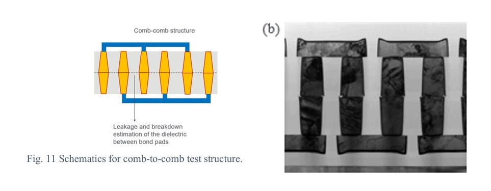
Source: Y. Trickett et al. “First Demonstration of 450nm Pitch Cu-Cu Hybrid Bonding with 98% Yield Across 20M Interconnects for Ultra-Dense 3D Integration” ECTC 2026
DOEs and yield vehicles such as comb structures and via chains are very common to analyze the effect of process parameters from IV curves and SEM images. Note that DOEs often consume a lot of tool and engineering time to do the analysis to determine the proper fab recipes, making these recipes highly guarded IP.
A Step-by-Step Overview of the Hybrid Bonding Process: Surface Preparation and Annealing
The detailed process flow goes something like this:
Surface Preparation
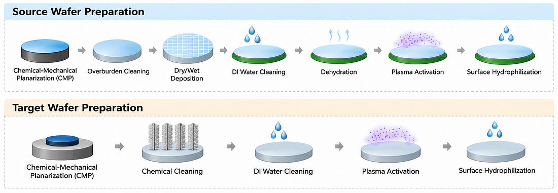
The surface of the die must be flattened, cleaned, and properly activated. Surface preparation involves the following steps:
- CMP. Both source and target wafer undergo chemical cleaning and mechanical polishing. CMP recesses the copper from the surface of the oxide.
- Singulation. The source wafer is singulated (for D2D/D2W) where a metal saw, plasma, or laser cuts the wafer along scribe lines.
- DI Wafer cleaning. De-ionized water removes stray particles that singulation may have caused.
- Degassing (optional). The source die is degassed to remove water trapped in the ridges of the scribe lines.
- Plasma Activation. The dielectric surface is exposed to a plasma (O2, N2, or Ar) to remove organic residues and create a uniform surface of “dangling bonds”.
- Surface Hydrophilization. The activated surface is exposed to deionized water to chemically prepare the surface for room temperature oxide bonding.
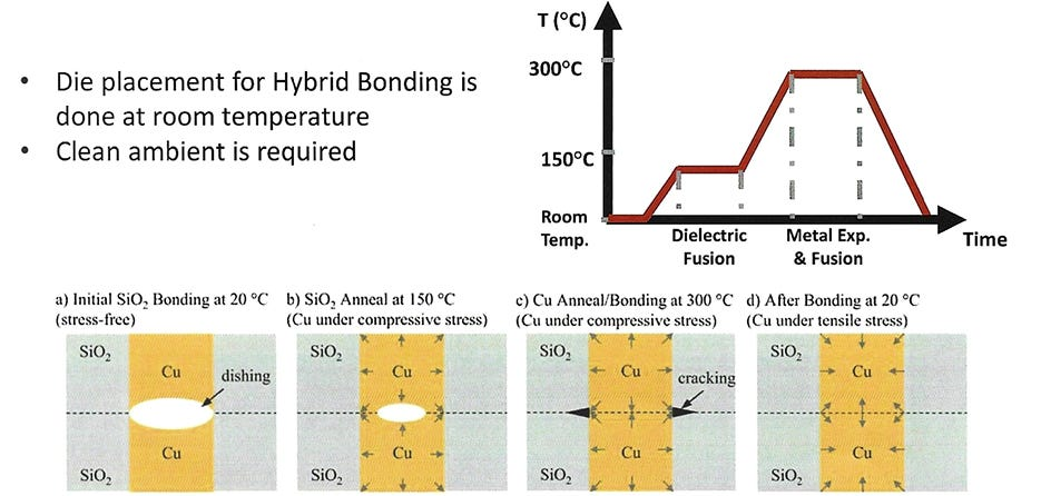
The two surfaces are then aligned and brought together at room temperature where the initial bonds form and fixes the die into position. Self alignment using water droplets is a promising alternative, with Intel and CEA Leti working on its development to improve throughput by up to 10x.
Annealing
Source: I. Pachenko et al. “Microstructure Development of Cu/SiO2 Hybrid Bond Interconnects after Reliability Tests” IEEE Transactions on Components, packaging, and manufacturing technology, vol. 12, no. 3, 2022.
Then, the bond goes through an annealing process. A representative temperature profile can look like the following:
- 150o C to anneal the SiO2 surface together, strengthening the oxide bond
- 300o C to anneal the copper, causing it to expand under compressive stress
- Lower the temperature back down to 20o C
These temperatures are not set in stone and depend on several material factors. Cu-Cu annealing can be performed as low as 200o C, but bonds generally form more slowly and require tighter Cu recess control.
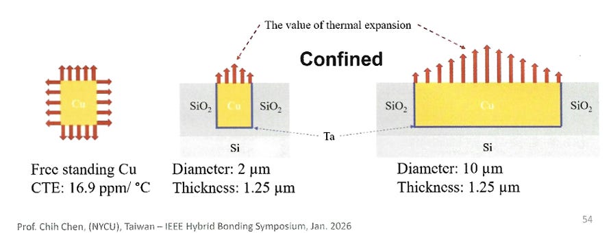
There are a few important nuances about the copper pads:
- The “effective” vertical displacement of Cu depends on the dimensions of the Cu pads. Cu is confined on the side walls and a larger diameter pad can force more of the copper material to go up.
- Pad layouts can have a significant impact on hybrid bonding yield. Designers should balance pad redundancy and performance benefits during early design stages.