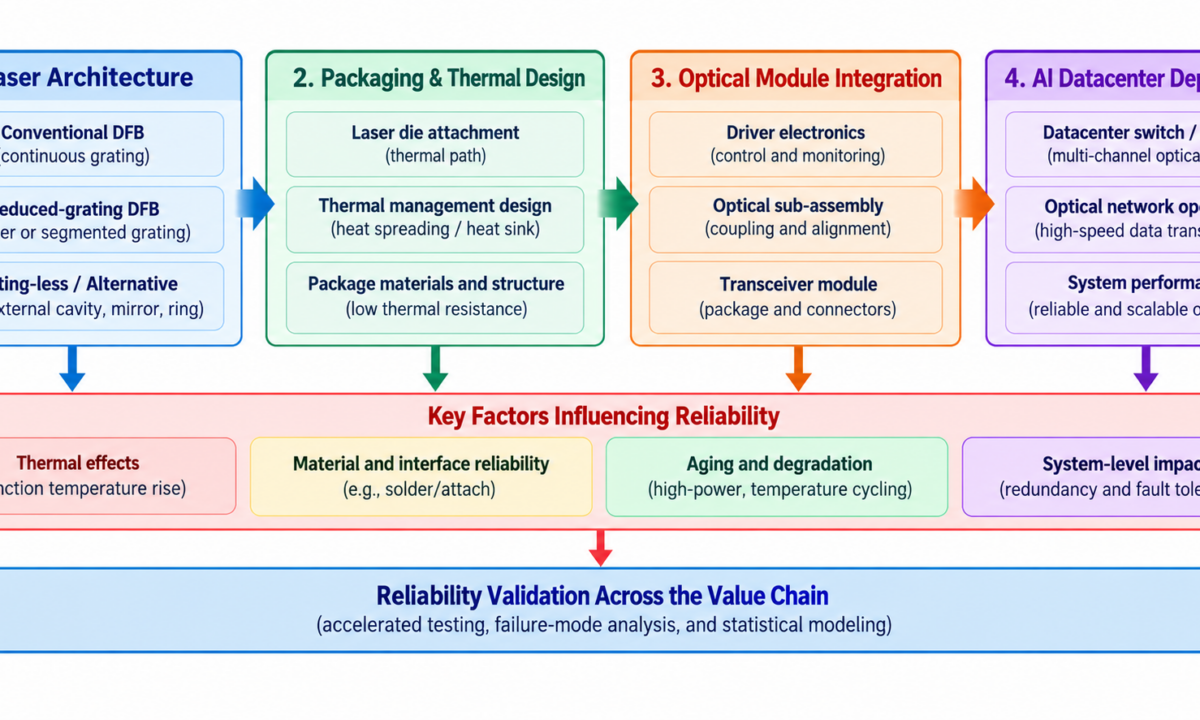
Who Is This For
This article is for photonics and semiconductor engineers, optical-module designers, reliability teams, datacenter-network architects, and technical leaders who are evaluating laser architectures for high-power AI interconnects. It assumes a working knowledge of DFB/DBR lasers, thermal impedance, side-mode suppression ratio (SMSR), and accelerated reliability testing.
Key Takeaways
• At AI-cluster scale, laser reliability becomes a system problem. A failed optical link can disrupt synchronized training traffic and reduce useful GPU time.
• Continuous gratings are a proven way to control laser modes, but etched and regrown structures bring fabrication and thermal trade-offs that matter more as power density rises.
• Grating-less and reduced-grating designs are worth exploring when they can maintain spectral control while simplifying the active region and improving thermal uniformity.
• COMSOL or similar multiphysics tools can help connect optical, electrical, and thermal behavior before fabrication. Any claimed improvement, however, should be backed by clearly documented model geometry, materials, boundary conditions, mesh sensitivity, and measured correlation.
• Reliability improvements should be supported by accelerated-life testing, failure-mode analysis, and a documented statistical model before they are presented as demonstrated outcomes.
1. The Reliability Problem Hidden Inside AI Scale
In a large AI cluster, the optical fabric is not just supporting the compute system. It is part of the compute path itself. NVIDIA has publicly described 100,000-GPU systems built around high-performance scale-out networking, which gives a sense of how quickly link count and network dependence grow at hyperscale [1]. At that scale, the semiconductor lasers inside optical transceivers become an important part of overall system reliability.
So the real engineering question is not simply whether a laser meets its optical specification when it leaves the lab. The harder question is whether it can keep meeting that specification through high output power, temperature cycling, and long duty cycles, especially when even a small failure rate is multiplied across hundreds of thousands or millions of optical links.
One failed component will not necessarily stop an entire cluster because modern systems can use redundancy and recovery mechanisms. Still, a failure may trigger link retraining, traffic rerouting, checkpoint recovery, maintenance, or job interruption. At AI scale, reliability differences that look small at the device level can become meaningful at the system level.
2. Re-examining Continuous Gratings
Distributed Feedback (DFB) lasers use periodic refractive-index modulation to provide wavelength-selective feedback and strong longitudinal-mode discrimination. The architecture is mature, well understood, and widely deployed. The reason to revisit it is not that continuous gratings are inherently unreliable. Rather, some of their design and fabrication trade-offs can become more important as optical power density and thermal loading increase.
In many DFB implementations, forming the grating and then performing epitaxial regrowth adds process complexity. Etch uniformity, interface quality, geometry, current distribution, optical-field distribution, and heat flow can influence one another. At higher power, it makes more sense to evaluate these factors as a coupled system than as isolated specifications.
Established strengths of continuous-grating DFB designs
• Strong longitudinal-mode discrimination and stable single-mode operation.
• Narrow linewidth and wavelength control suitable for dense optical systems.
• Decades of manufacturing experience, qualification history, and foundry process knowledge.
Design risks to evaluate at high power
• Thermal non-uniformity: localized absorption, current crowding, or geometric discontinuities can raise the peak junction temperature even when the average package temperature still looks acceptable.
• Regrowth and interface quality: etched-and-regrown structures add process sensitivities that need careful control through epitaxy, metrology, and qualification.
• Fabrication tolerance: grating geometry directly affects coupling and spectral behavior. For example, COMSOL studies of laterally coupled DFB structures show that grating dimensions and duty cycle influence both performance and fabrication tolerance [2].
3. Engineering an Alternative: Grating-Less or Reduced-Grating Architectures
A grating-less design replaces a continuous periodic structure in the active region with another form of wavelength selection or optical feedback, such as localized feedback features, engineered facets, external reflectors, or other precision structures. The goal is not to remove the grating for its own sake. It is to keep the required spectral behavior while reducing process steps or structural features that may add thermal or manufacturing sensitivity. A reduced-grating design takes a middle path: it keeps the grating only in selected regions, or over a shorter interaction length, instead of extending it across the full active region.
The idea behind this approach is simple. A more uniform active region may produce a more uniform current-density and temperature profile. But that benefit cannot be assumed. It depends on the full device design, including the epitaxial stack, contact resistance, cavity geometry, facet coatings, package thermal resistance, and operating conditions [6, 7]. The advantage has to be demonstrated in the complete device.
Advanced lithography can define localized optical features with high precision. Even so, an alternative architecture still has to earn its place. It must match or improve the conventional DFB/DBR baseline in SMSR, wavelength stability, efficiency, modulation performance, manufacturability, and lifetime.
4. Validation Through Multiphysics Simulation
Moving from a conventional grating design to an alternative architecture requires more than a good physical argument. The design should first be tested with coupled optical-electrical-thermal modeling and then checked against physical devices. COMSOL provides semiconductor, wave-optics, and heat-transfer capabilities that can be combined for optoelectronic-device analysis [3]. Its heat-transfer tools model thermal conductivity and temperature fields, while its wave-optics tools can resolve wavelength-scale structures [3][4].
For the comparison to mean anything, the baseline and proposed designs should use the same package assumptions and operating points. At minimum, the analysis should document the epitaxial stack and material properties, drive current or optical-output target, heat-source assumptions, thermal boundary conditions, mesh convergence, and the metrics used to compare the designs.
Recommended simulation outputs
• Peak active-region temperature and junction-to-reference thermal resistance or impedance.

• Current-density and carrier-density uniformity across the active region.
• Optical-field and photon-density profiles, including sensitivity to fabrication tolerances.
• Wavelength shift and SMSR across temperature and drive current.
• Threshold current and efficiency at matched operating points.
Reporting Simulation Results
Any quantitative improvement reported for an alternative architecture should be accompanied by the model definition, boundary conditions, material assumptions, mesh-convergence analysis, and correlation with physical measurements. Thermal performance should be reported using the actual modeled quantity, such as junction temperature or thermal resistance, rather than a broader metric that may not accurately describe the simulation output.
5. Reliability Validation: From Device Physics to Accelerated-Life Testing
Reliability claims are only useful when the assumptions and evidence behind them are clear. Telcordia GR-468-CORE describes reliability-assurance practices for optoelectronic devices, including laser diodes and modules [5]. The important point for this discussion is that reliability should be demonstrated through accelerated aging, qualification testing, failure-mode analysis, and appropriate statistical methods rather than inferred from the device architecture alone.
At datacenter scale, even relatively infrequent component failures can become operationally significant because a system may contain hundreds of thousands or millions of optical links. The actual system impact depends on redundancy, correlated failure modes, repair time, traffic architecture, and the number of laser devices in each link. For that reason, device-level reliability results should be connected carefully to system-level availability rather than reduced to a single projected failure-rate number.
What reliability evidence is needed
A grating-less or reduced-grating design should not be described as more reliable solely because its thermal profile appears more uniform in simulation. A defensible reliability case requires accelerated aging, clearly defined stress conditions, failure-mode analysis, appropriate statistical treatment, and correlation with physical devices. Where quantitative reliability results are presented, the test methodology and assumptions should be visible to the reader.
6. What Must Be Proven Against the Baseline
A grating-less design becomes interesting only if it improves measurable engineering outcomes without giving up the properties that made DFB lasers successful in the first place. That is why the comparison should be built around a controlled baseline, not broad claims about “legacy” technology.
| Metric | Conventional DFB/DBR baseline | Alternative architecture: evidence required |
| Spectral performance | Established mode control; quantify SMSR and wavelength drift | Show equal or better SMSR and stability over current and temperature |
| Thermal behavior | Measure junction temperature and thermal impedance | Show lower peak temperature or thermal impedance under matched output power |
| Efficiency | Measure wall-plug/slope efficiency at matched conditions | Demonstrate improvement or no material penalty |
| Manufacturing | Mature but process-dependent grating/regrowth flow | Demonstrate yield, tolerance window, repeatability, and cost |
| Reliability | Qualification history available for mature designs | Demonstrate COD margin, accelerated aging, accelerated-life performance and statistical confidence |
7. Conclusion: Make Reliability a Measured Design Variable
AI datacenters are pushing bandwidth, power efficiency, and availability at the same time. That is a good reason to take a fresh look at semiconductor-laser architectures, including designs that reduce or eliminate continuous gratings. But the case for changing the architecture will ultimately be made by data, not by rhetoric.
The practical path is clear: define a conventional baseline, model both architectures under the same conditions, fabricate representative devices, and compare the simulations with thermal, spectral, and accelerated-life measurements. If an alternative layout can show lower junction temperature, stable SMSR, competitive efficiency, manufacturable tolerances, and a statistically supported reliability improvement, it has a credible case for AI-scale optical infrastructure. Until that evidence is available, quantitative reliability improvements should be presented cautiously, with the assumptions and validation methods visible to the reader.
About the Author
Akshitha Gadde is a semiconductor and photonics R&D engineer with more than 10 years of experience in semiconductor lasers, photonics, and optical communication technologies. Her work focuses on high-power laser design, DFB/DBR architectures, semiconductor reliability, and the use of simulation tools to understand photonic-device performance and reliability. She has contributed to semiconductor product development, research, and patent-related work throughout her career.
The views expressed in this article are the author’s own. This article is an independent technical contribution and is not affiliated with, sponsored by, or endorsed by the author’s current or former employers.
References
[1] NVIDIA, “NVIDIA Ethernet Networking Accelerates World’s Largest AI Supercomputer, Built by xAI,” Oct. 28, 2024. Describes a 100,000-GPU Hopper cluster using Spectrum-X Ethernet. https://nvidianews.nvidia.com/news/spectrum-x-ethernet-networking-xai-colossus
[2] R. Millett, A. Benhsaien, K. Hinzer, T. Hall, and H. Schriemer, “Simulation of Fourth-Order Laterally-Coupled Gratings,” COMSOL Conference, 2008. https://www.comsol.com/paper/simulation-of-fourth-order-laterally-coupled-gratings-4983
[3] COMSOL, “Semiconductor Module: Simulate Semiconductor and Optoelectronic Devices.” https://www.comsol.com/semiconductor-module
[4] COMSOL Documentation, “Heat Transfer in Solids” and Wave Optics / grating modeling documentation. https://doc.comsol.com/6.3/doc/com.comsol.help.comsol/comsol_ref_heattransfer.30.25.html
[5] Telcordia Technologies, GR-468-CORE, “Generic Reliability Assurance Requirements for Optoelectronic Devices Used in Telecommunications Equipment,” Issue 2. The standard outlines reliability-assurance and accelerated-aging practices for optoelectronic devices.
[6] S. N. Mohammad, “Sampled Grating Distributed Feedback (SG DFB) Semiconductor Laser Diode,” Optics & Laser Technology, vol. 39, no. 4, pp. 754–757, 2007.
[7] S. Tang, L. Hou, X. Chen, and J. H. Marsh, “Multiple-Wavelength Distributed-Feedback Laser Arrays with High Coupling Coefficients and Precise Channel Spacing,” Optics Letters, vol. 42, no. 9, pp. 1800–1803, 2017.