Modern flat-panel displays depend on highly complex multilayer structures fabricated on enormous glass substrates. As display generations continue to grow, lithography must combine large-area processing with increasingly demanding requirements for resolution, uniformity, and alignment.
One technology that helps simplify this process is the halftone photomask (HTM). By combining opaque and partially transmissive regions on a single mask, halftone lithography can create different photoresist thicknesses in one exposure, enabling multiple processing steps within a simplified mask flow.
Why Display Manufacturing Needs New Lithography Approaches
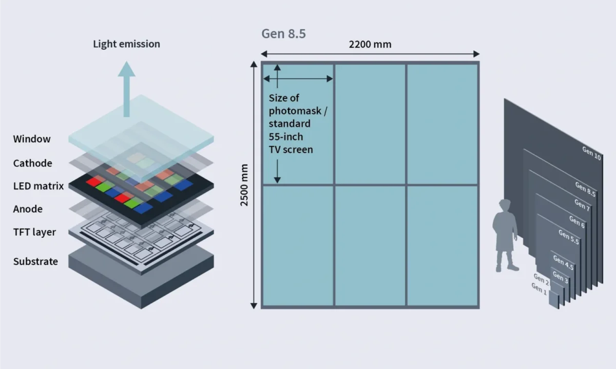
An active-matrix OLED (AMOLED) display consists of multiple functional layers. The backplane contains a thin-film transistor (TFT) circuit that controls the individual sub-pixels, while the frontplane contains the light-emitting components. Building a complete display can require 20 or more individual photomasks across the overall manufacturing process.
The scale of the substrates makes this particularly challenging. In Gen 8.5 display manufacturing, for example, mother glass can measure approximately 2200 × 2500 mm, with six 55-inch TV panels fitting onto a single substrate. At these dimensions, photomasks themselves become very large and expensive, while every lithography step must maintain tight registration and uniformity across the entire area.
Reducing the number of lithography steps can therefore improve both throughput and manufacturing economics.
This is where halftone photomasks come into play.
How Does a Halftone Photomask Work?
A conventional binary photomask typically consists of transparent quartz with opaque chrome areas defining the pattern. A halftone photomask adds a partially transmissive layer, such as a chromium oxide compound, whose optical properties can be precisely engineered.
The partially transmissive layer performs two important functions.
First, its thickness can be engineered to produce a phase shift relative to the surrounding quartz. This creates destructive interference at pattern boundaries, helping produce sharp, high-contrast resist features while also increasing the depth of focus and widening the process window.
Second, its composition can be adjusted to control optical transmission. For display photomasks, transmission is typically tuned within a range of around 20–50%.
The result is a key advantage: a single exposure can generate multiple resist thickness levels.
Creating Multiple Resist Levels in One Exposure
After exposure through a halftone photomask and development, a positive photoresist can contain three distinct regions:
- Full resist thickness where the mask is opaque
- Reduced resist thickness where light is partially transmitted through the halftone region
- Zero resist where the mask is fully transparent
This stepped resist profile makes it possible to perform different subsequent processing operations using a single lithography step.
In display manufacturing, halftone photomasks are commonly used in a four-mask TFT process flow. One important application is the simultaneous definition of the active semiconductor channel and the source/drain metal contacts.
After exposure, sequential etching and resist-thinning steps selectively remove the relevant material layers. Because the critical structures originate from the same mask exposure, the resulting features are inherently self-aligned, eliminating alignment errors between the channel and contacts across the large glass substrate.
That combination of process simplification and self-alignment is one of the key attractions of halftone lithography for large-area displays.


The Challenge: Manufacturing the Photomask Itself
The advantages of halftone lithography come with demanding requirements for the photomask manufacturer.
Fabrication starts with a large glass substrate onto which the partially transmissive halftone film and opaque chrome layer are deposited. Conventional spin coating is no longer practical at these dimensions, so techniques such as slit coating are used. Laser lithography then patterns the substrate, followed by development and highly controlled etching of the different layers.
The required performance is substantial: For advanced display photomasks, a critical-dimension uniformity below ±50 nm across large substrates is necessary, together with overlay accuracy typically better than 500 nm over meter-scale areas. Defect control is equally important because even small mask defects can affect the resulting display manufacturing process.
These requirements make the accuracy and stability of the mask-writing system critical.
VPG⁺ 1400 FPD / VPG⁺ 1850 FPD: Precision at Display Scale
To address the overlay and uniformity challenges associated with multilayer halftone photomask fabrication, Heidelberg Instruments developed the VPG⁺ 1400 FPD / VPG⁺ 1850 FPD for next-generation display applications.
The systems combine a large writing area with a stable mechanical and thermal environment. They feature a write area of up to 1400 × 1800 mm², a granite chuck, and a temperature-controlled environmental chamber designed to mitigate thermal runout on large substrates. Tool-matching capabilities compensate for differences in coordinate systems between mask-writing tools, including offsets, rotation, scaling, and distortion.
At the heart of the exposure system is a high-speed Grating Light Valve (GLV) combined with a 355 nm DPSS laser and a custom double-coated write lens. The optical engine provides an 8 nm address grid and a minimum written feature size of 800 nm, with a throughput of 2750 mm²/min. For a 1200 × 1400 mm photomask used for G8 display panels, this corresponds to an exposure time of approximately 10 hours.
For halftone mask manufacturing, however, throughput alone is not enough. The second exposure layer must be positioned precisely relative to the opaque chrome pattern underneath it.
The VPG⁺ platform addresses this with a through-the-lens alignment camera, which measures the substrate position directly through the exposure optics. This creates a fixed relationship between metrology and exposure. The architecture can additionally be supported by image recognition and a 1 nm interferometric position-control system. This enables second-layer alignment with a mean + 3σ of 400 nm across a 1000 × 1000 mm² area.

Why Halftone Photomasks Matter for the Future of Displays
As display manufacturing scales to larger substrates and increasingly sophisticated devices, every additional lithography step adds cost, time, and opportunities for alignment errors.
Halftone photomasks offer a way to create multiple resist levels in a single exposure while enabling self-aligned processing of critical TFT structures. For mask manufacturers, this in turn places exceptional demands on CD uniformity, overlay, defect control, and large-area thermal stability.
The development of suitable mask-writing technology is therefore an important part of enabling the next generation of large-area displays.
Want to explore the topic in more detail?
Read the full article, “Halftone Photomasks: Enabling Flat Panel Display Manufacturing,” in issue 4 of The Lithographer: From Lab to Fab.