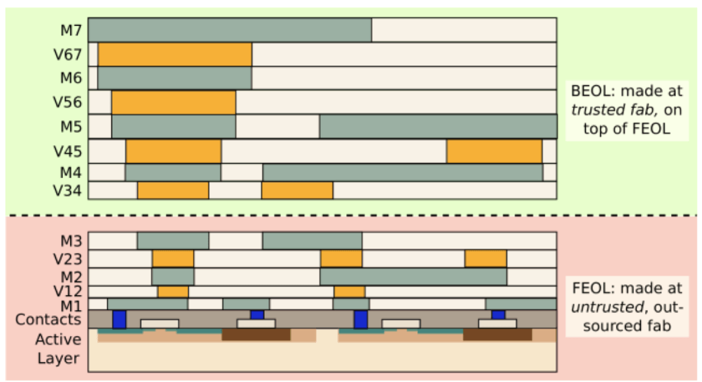
Figure 3: Front-end and back-end of a wafer processed separately, in different wafer fabs, to protect IP.