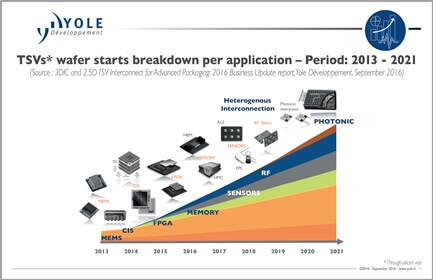
This year again, both market segments, high end, and low end, are the main targets of through silicon via (TSV) technology providers. In its latest advanced packaging technology and market analysis entitled 3DIC and 2.5D TSV Interconnect for Advanced Packaging: 2016 Business Update report, Yole Développement (Yole) announces, high volume production started: 3D TSV is a reality, especially in the memory industry… Amongst a dynamic advanced packaging market showing an overall advanced packaging revenue CAGR estimated at 8%, rising to US$ 30 billion in 2020. The development of TSV platforms is still pushed by the need to increase performance, functionalities, and integration; in addition, form factor and cost reduction are also part of the playground.
The More than Moore market research and strategy consulting company presents an overview of the 3D/2.5D IC packaging technologies per application. In addition to wafer forecast for 2015-2021 for different TSV applications, Yole’s analysts review the status of the current and future 3D IC products. They also describe and analyze the dedicated technology roadmap per device and highlight the organization of this market including supply chain activities, a list of key players and OSAT and foundry strategies.
3D TSV technology is becoming a key solution platform for heterogeneous interconnection, high-end memory and performance applications.
The higher end market segment is led by 3D stacked memories, 2.5D integration and emerging application such as photonics. From its side, the low-end application includes CMOS image sensor (CIS), microelectromechanical systems (MEMS) devices and other sensors and new applications such as LEDs.
TSVs have now become the preferred interconnect choice for high-end memory. They are also an enabling technology for heterogeneous integration of logic circuits with CIS, MEMS, sensors, and radio frequency (RF) filters. In the near future, they will also enable photonics and LED function integration.
“The market for 3D TSV and 2.5D interconnect is expected to reach around 2.1 million wafers in 2021, expanding at an 18% CAGR,” asserts Santosh Kumar, Senior Technology& Market Analyst at Yole. The growth is driven by increased adoption of 3D memory devices in high-end graphics, high-performance computing, networking and data centers, and penetration into new areas, including fingerprint and ambient light sensors, RF filters, and LEDs.
CIS still commanded more than 80% share of TSV market wafer volume in 2015, although this will decrease to around 56% by 2021. This is primarily due to the growth of the other TSV applications, led by 3D memories, RF filters, and fingerprint sensors. However, hybrid stacked technology, which uses direct copper-copper bonding, not TSVs, will penetrate around 38% of CIS production by 2021. The TSV markets for RF filters and fingerprint sensors are expected to reach around US$2.6 billion and US$0.7 billion by 2021 respectively.
Under this new report, Yole’s analysts also highlight the diversity of business models within the 3D & 2.5D TSV supply chain. They identify:
Integrated devices manufacturers (IDMs) with Samsung, Micron, Freescale, Sony, Toshiba, STMicroelectronics
Outsourced semiconductor assembly & test companies (OSATs) including SPIL, Amkor Technology, ASE, Powertech
- CMOS foundries with TSMC, SMIC and more.
Si interposers suppliers, 3D packaging foundries, and R&D services are also part of the business models identified by Yole’s analysts.
So will 3D TSV open the doors for new strategies? Indeed each player has its own approach:
- Both OSATs, Amkor Technology and SPIL are strongly involved in the memory and the MEMS & Sensor market.
- In parallel Samsung, an IDM is well positioned in the CIS, Si interposer and LED market segments only.
- In addition, no foundries for memory products have been identified by Yole’s advanced packaging team.
Amongst the numerous 3D & 2.5D TSV players, Micron, SKHynix, Samsung, AMS and Avago Technologies are investing in CapEx. A detailed analysis per player is available in Yole’s report, especially the OSATs and foundries strategies, that are willing to increase their market shares for TSV applications.
According to Yole’s analysts, 3DIC & 2.5D TSV continue its attractive growth. Under a dynamic ecosystem, a lot of valuable companies are involved in this field and propose innovative solutions. Because of the increasing consumer market, as well as the need for higher performance products such as 4K gaming, networking, 2.5D/3D TSV packaging platform becomes a key solution platform.
During the Electronics Packaging Technology Conference (EPTC) taking place from November 30 to December 3 in Singapore, Yole’s expert, Santosh Kumar will present his vision of the 3DIC & 2.5D TSV industry. His presentation is entitled: “What’s happening in TSV based 3D/2.5D IC packaging: Latest market & technology trends”. Discover the program and register on EPTC 2016.
More detailed information about Yole’s report is available on i-micronews.com, advanced packaging reports section.
Source: http://www.yole.fr


![[err-ad-fallback-title]](http://www.3dincites.com/wp-content/plugins/a3-lazy-load/assets/images/lazy_placeholder.gif)


