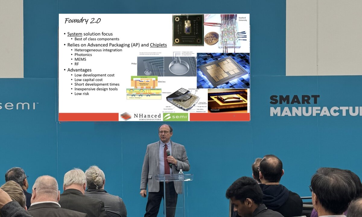
NHanced Semiconductor president Robert Patti’s presentation at the recent SEMIEXPO Heartland in Indianapolis, IN described the critical role of advanced packaging in continuing the progress of Moore’s Law in semiconductor development. Following is a summary of his presentation.
In Gordon Moore’s seminal paper, he predicted a ‘Day of Reckoning’ for semiconductor scaling. That day has arrived. However, as predicted, there is another path forward for semiconductors to continue progress without relying solely on ever-shrinking devices. Advanced packaging is that new path, and it is at the heart of a new industry model known as Foundry 2.0.
Moore’s Law (a prediction that the number of transistors on a chip would double every two years) was not primarily about scaling; first and foremost, it was a statement about economics. The foundational premise was that the industry could shrink transistors and build more of them for the same cost, and this was true for the past 50 years. However, this is no longer the case, because although nominal transistor size can indeed shrink further, the cost per transistor no longer declines.
As a result, the semiconductor industry is facing a sea change from the traditional “Foundry 1.0” model, which is focused on high volume production of chips. This model entails high development and capital costs, long development times, expensive design tools, and high risk. A new business model is needed to continue the performance and the economics of Moore’s Law.
The new business model, pioneered by NHanced Semiconductors, is Foundry 2.0 – sourcing best-of-class components from traditional foundries and employing advanced packaging and additive manufacturing methods to create highly customized assemblies with superior performance and lower costs. Foundry 2.0 represents a system approach to semiconductor manufacturing, using advanced packaging techniques such as heterogeneous integration, low-temperature hybrid bonding, and silicon or glass interposers to incorporate photonics, MEMS, and RF devices.
This foundry evolution delivers lower development costs, lower capital costs, shorter development times, less expensive design tools, and less overall risk than traditional semiconductor manufacturing. Foundry 2.0 fundamentally changes the market to a lower volume, high mix manufacturing model, providing more cost-effective semiconductor procurement opportunities for US government agencies, technology startups, and specialized markets that require fewer transistors per device. Because Foundry 2.0 uses components manufactured in traditional foundries, its capital costs for design tools and production equipment are orders of magnitude lower, and the cost of the resulting components can be reduced by 10x to 50x.
Another key technology for the Foundry 2.0 transition is the chiplet – a bare die with a well-defined subset of functionality, designed to be combined with other chiplets in any number of different applications. Chiplets provide standardized building blocks that offer reuse of specific functionality, delivering advanced packaging assemblies with NRE costs ~100x lower than those of leading-edge semiconductor nodes. With recent advances in hybrid bonding, chiplet-to-chiplet power connections and delay times are comparable to on-die performance. Most importantly, chiplets enable manufacturers to target niche markets by using only necessary transistors, instead of the “one size fits all” approach of conventional SoCs.

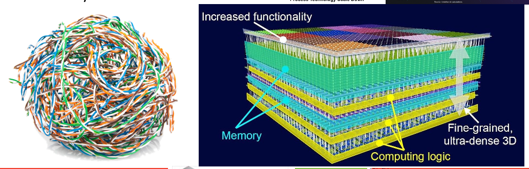
The use of chiplets and 2.D / 3D architectures provides fundamental advantages by dramatically reducing the wiring (metallization) interconnections within advanced packaging assemblies. These shorter interconnections mean less signal delay. Also, because memory retrieval functions account for the majority of power usage within the assembly, 3D architectures with shorter interconnects reduce power usage.
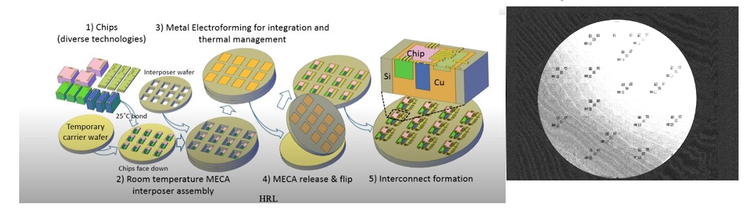
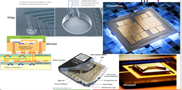
Another technology innovation driving the advanced packaging evolution is heterogeneous integration – the ability to combine dissimilar chips in a single device. This includes combining alternative semiconductor materials with conventional silicon CMOS. In 3D packaging, the various tiers may be made of different materials. In 2.5D packaging, interposers accommodate the differences in CTE (coefficient of thermal expansion), alignment accuracy, and processing temperature to present a single interface to the organic substrate. This enables the assembly designers to integrate “best-in-class” materials (III-V devices, photonics, RF and analog devices, and MEMS technologies) in a way that cannot be achieved with monolithic semiconductor processes.
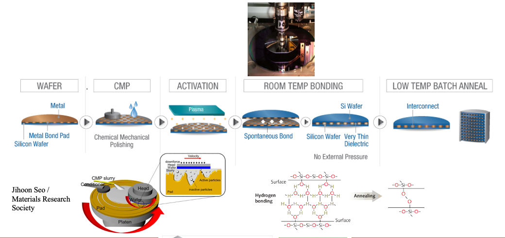
Direct Bond Interconnect (DBI®), a type of low temperature hybrid bonding, is a precision process that permanently bonds the surfaces of two wafers, dies, and/or chiplets. It is called “hybrid” because it combines two distinct types of bonds at the interface: a dielectric-to-dielectric covalent bond and a metal-to-metal fusion bond. DBI hybrid bonding is a critical technology for 2.5D and 3D advanced packaging. It creates a seamless bond and enables extremely fine-grained interconnect. The bonded parts behave like a single circuit without the need for ESD structures. Advantages of this bonding technique include lower capacitance (translating to lower power and higher speeds), a rugged hermetic seal for extreme environments, and a seamless metal bond at fine interconnect pitches for abundant bandwidth.
Conclusion: This evolution to Foundry 2.0 employs advanced packaging technology to create a manufacturing model inherently different from today’s traditional semiconductor foundry. The integration of heterogeneous components in 3D and 2.5D devices, the use of silicon and glass interposers, and leveraging of chiplets for cost reduction and innovation represents a fundamental change in the semiconductor industry. NHanced Semiconductors is the first US-based pure-play advanced packaging foundry to employ this revolutionary Foundry 2.0 business model.