
Continuing our coverage of ECTC 2021, let’s take a look at the session on Heterogeneous Integration (HI) using 2.XD/3D packaging, chaired by Subash Shinde of Notre Dame and John Knickerbocker of IBM.
IBM Introduces Direct Bonded HI Si Bridge Technology
Though they are not manufacturing chips or packages anymore, IBM R&D has been busy simplifying what we have come to call embedded bridge technology. Kamal Sikka of IBM discussed IBM’s direct bonded heterogeneous integration (DBHi) SI Bridge technology.
As can be seen in Figure 1, there is a direct copper pillar connection between chip A and chip B through a silicon bridge. That subassembly is joined to a laminate chip carrier with a standard C4 pitch.
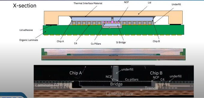
The major difference between this and the Intel EMIB technology is that the chips are attached to the laminate with standard C4 bumps and the bridge is connecting the chips or chiplets with micro bumps formed on the bridge side. There is no need for multiple pitch bumps on the same device (chip or bridge) as there is in EMIB. The laminate substrate bond and assembly supply chain is not altered. This is significant and is an issue IFTLE has brought up several times when discussing the Intel technology (not for the faint of heart). Wafer fabrication of the chips that are connected by the bridge is shown in Figure 2.
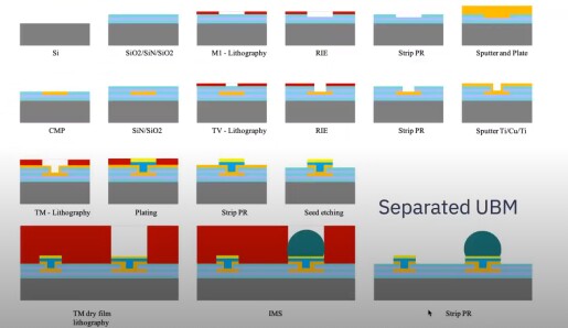
The bridge is fabricated by a standard wafer fab process. The chips have to go through a tw0-pass soldering process. Once the pads are plated they do a second dry film resist and the bump is deposited by the IBM IMS process.
In terms of the process sequence, shown in Figure 3, chips A and B are first joined to the bridge by thermocompression bonding, inverted and the C4 bumped chips A and B are joined to the laminate substrate with the bridge slipping into a trench that is created in the correct position on the laminate. So, this is a chips-bridge-first assembly process.
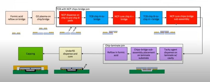
Since the trenches are so small, there is little impact on laminate warpage during processing. The process did need optimization to minimize NCP entrapment between the joining surfaces. The underfill step proved to be important. Underfill had to enter the trench to anchor the bridge or the packages “were not reliable”.
TSMC’s Advanced Chiplet Integration
Terry Chang discussed integrated fan-out on substrate (InFOoS) technology for advanced chiplet integration. InFOoS is an InFO-based technology for the integration of chiplets for 5G network applications. It offers 2/2µm L/S and micro bumps on 40µm pitch on up to 1.5X reticle size. InFOoS has been in production since 2018. Hen compared it to a more standard multi-chip module (MCM) technology with 15µm L/S (Figure 4). It reveals 7X better bandwidth/mm.
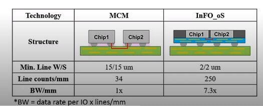
Figure 5 shows how a test vehicle was fabricated for a 10 chiplet module with 2.5X reticle size substrate.
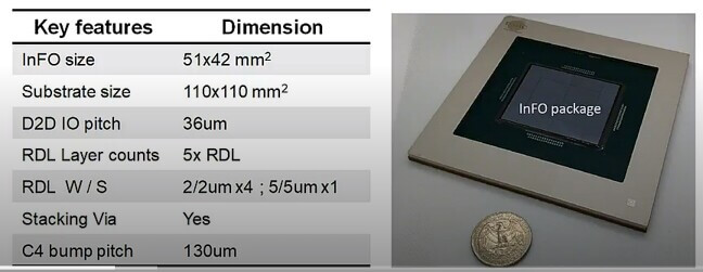
There were > 60k IO connected through the 2/2 L/S RDL. A 95% wafer-level yield was demonstrated.
Warpage at 250°C of the 2.5X reticle module was found to be 3X that or a 1X reticle-sized module.
Stacked vias showed lower insertion loss and lower impedance than staggered vias. Simulation models showed that strain on corner bumps would be decreased 28% by using a low coefficient of thermal expansion (CTE) core substrate and a ring-type heat spreader. Such packages passed all standard JEDEC reliability tests such as HAST, high-temperature storage, and thermal cycling.
HRL Labs Chiplet in Wafer Technology
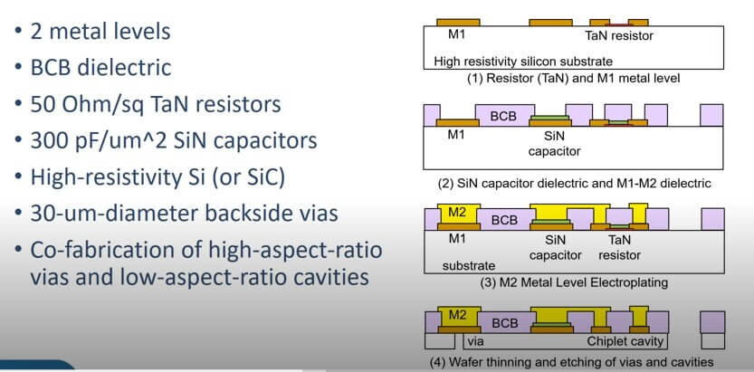
HRL’s Florian Herrault discussed chiplets-in-wafer (CiW) as a demonstration of high-frequency circuits with GaN chiplets in silicon interposers using their metal embedded chiplet assembly for microwave ICs (MECAMIC) technology.
III/V wafers are expensive and are used inefficiently since the area actually used for transistors is a small fraction of the area used to form the complete circuit. Therefore, breaking such circuits up into chiplets and using the III/V such as GaN only for the transistors could create a cost/performance paradigm.
For MECA, chips are embedded in a metallic heat spreader (copper) as shown in Figure 6. Basically, a reconstructed wafer with the chips embedded in copper instead of a mold compound.
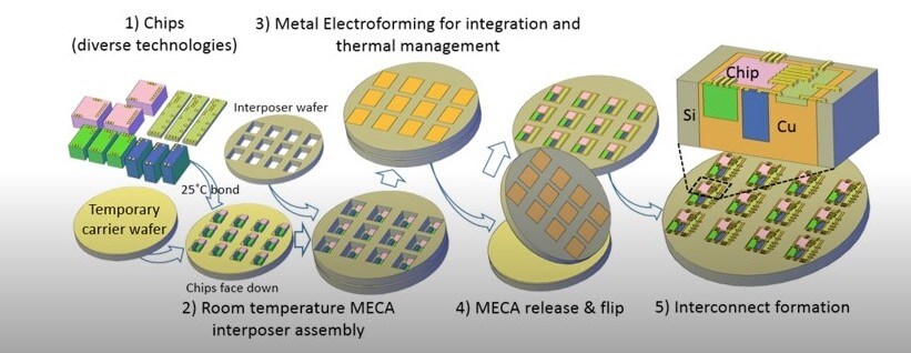
MECAMIC uses prefabricated III/V chiplets embedded in 300mm silicon wafers making efficient use of the expensive compound semiconductor materials. The circuit process flow is shown in Figure 6.
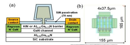
GaN chiplets for insertion into the silicon cavities to complete the Rf circuits are fabricated using the HRL T3 process. They are achieving ~ 50K GaN chiplets on a 100mm GaN Wafer at a yield of ~ 70%. A GaN chiplet is shown In Figure 7.
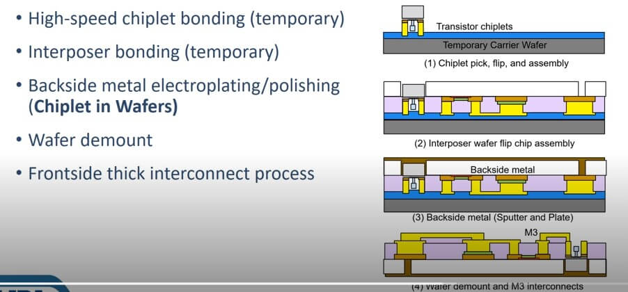
Chiplet assembly is shown in Figure 8. The chiplet is placed on a temporary carrier; the interposer is bonded; connections ae made and the temporary substrate is removed.
If such technology proves to be a manufacturable sequence, this could have a major impact on the cost of Rf and microwave circuits.
For all the latest in Advanced packaging stay linked to IFTLE……………………………………