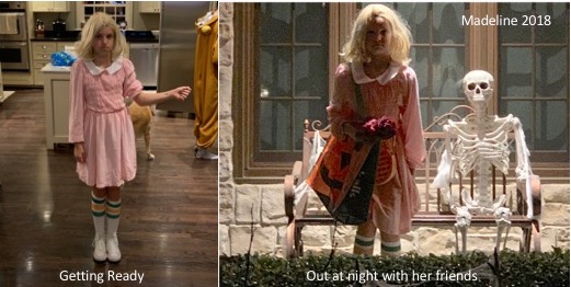
Who was Madeline on Halloween? Before we start more tech coverage of IMAPS 2018 with a look at polymer dielectric advancements, long time readers know that you are due a Halloween update on my granddaughters. This year I’m focusing on Madeline who will be eleven in February. Her Halloween disguise this year was from her favorite Netflix TV show. Can you guess the character and the show?? I have given you a big hint.
Continuing our look at IMAPS – Pasadena
It would not be an overstatement to say that the polymer dielectric advances of the past 25 years have made redistribution layers (RDL) possible and thus the entirety of wafer-level and fan-out (FO) packaging.
In the early 1990s, a company named N-Chip, led by Bruce McWilliams, and David Tuckerman, attempted to create high-density interconnect for multichip modules (MCMs)— the forerunners to system-in-package (SiP)—using SiO2 dielectric similar to what was being used for inter-layer dielectrics (ILD). The effort didn’t get too far, one of the major obstacles being the lack of thick low-stress oxide.
R&D practitioners quickly turned to the available polyimides (PIs) which were being used by IBM, NEC, Fujitsu, Hitachi and other mainframe makers of the time. But PIs, while having excellent thermal stability and mechanical properties, were initially a failure in applications like wafer-level packaging (WLP) due to their high cure temperatures (normally > 400C), propensity for water absorption, and poor planarization.
This led to Dow Chemical commercializing benzocyclobutene (BCB) dielectrics, which cured at 250°C or less, had much less water absorption and excellent planarization as well as a Dk of 2.65. As the acceptance of WLP spread, the PI community modified their compositions compromising their mechanical properties for better properties in these other areas. Constant polymer dielectric upgrading over the last two decades continues into the present time, where FO packages incorporating molding compound as their base structure could not / cannot be teamed up with RDL dielectrics that cure over 400°C.
At the recent IMAPS conference in Pasadena some of the major dielectric players introduced new materials for such applications.
HD Micro
Dow and DuPont may have merged, but my understanding is that HD Micro continues to exist as a separate entity, now half-owned (I assume) by Dow/DuPont. If this is incorrect someone please let me know…
In his IMAPS paper “Novel Low Temp Curable Photo Negative tone PI with Higher Resolution and Reliability” Matsukawa of HD Micro noted that negative-tone PIs for applications such as FO-WLP require finer line/space (L/S) and that lithographic performance of the PIs has to be improved and lower cure temperatures developed in order to meet industry future requirements. Specifically, they are looking for materials capable of achieving 3µm vias in 5µm thick films / 5µm vias in 10µm films with excellent planarization, 2/2 L/S capability and a low (~ 200°C) cure temp.
Cured film properties of PI 1, their current low-temp cure product, and PI 2, the newly developed product with a new photo package are compared in the table below.
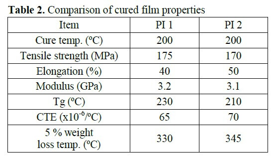 IFTLE has noted in the past that it makes all the difference in the world how these properties are measured. For instance, saying you are curing at 200°C does not tell the reader how much (if any) residual (uncrosslinked) functionality is left, which later could continue to react and give off water (steam) when the wafer is taken over 200°C. Also, thermal stability measured as “wt loss temp” should be measured isothermally, NOT by ramping the temperature and it is not clear here how that is being done in this case.
Their results do clearly show that regardless of cured thickness, PI 2 could be patterned at higher aspect ratio than PI 1 and they could reach their desired resolution specs. In addition, no failures of test samples were observed during 300 hr biased highly accelerated stress test (HAST). There is no statement on whether the PI 2 material is about to become commercial.
Taiyo Ink
Okamoto, of Taiyo Ink, in his presentation “New Photo Dielectric Material for High Density RDL with Ultra Small Photo Vias and High Reliability “ indicates that they are seeking high resolution, low coefficient of thermal expansion (CTE) and low residual stress for next-gen RDL, 2.5D interposer, and FO-WLP applications.

Their newly developed material, PDM, reportedly consists of carboxylic acid resin, photo acrylate resin, epoxy resin and fillers. It is sold as a film. Properties are shown below.
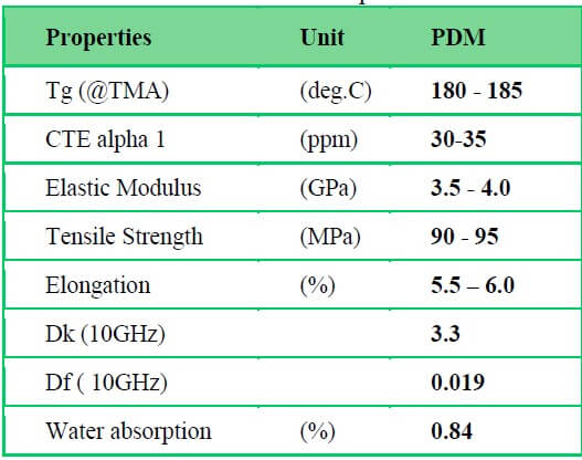
With a reported elongation of 5.5%, I would worry about its ability to resist cracking during and stress imposed situation. They were able to resolve 3µm vias in a 5µm film. Test structures reportedly passed -55 to + 125°C temp cycling.
MicroChem
Nawrocki of MicroChem described their “Novel Low Temp Curable Photo Patternable Polyamide with High Planarity for WLFO Packaging”. Their material known as KMRD is aqueous developable and reportedly cures at 185°C (2 hrs). Note this is a polyamide NOT a polyimide. Properties are compared to other dielectrics in the table below. They claim via patterning at aspect ratios ~ 1.5.

Toray
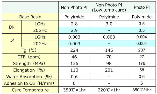
Tomikaawwa, of Toray, in their paper “Photo PI having Low Loss for Rf Applications”, indicates that low-loss PIs are required for 5G telecom and MM wave radars.
To obtain a low loss PI for Rf applications they investigated the impact of the PI structure and the photo package on the RF performance. They developed several PIs (photo vs non photo vs low temp curable) as shown in the table below.
IFTLE concludes from comparing these four papers that the perfect material is yet to be found and the best advice continuous to be to make your selection based on your specific requirements. AGAIN – IFTLE recommends care when comparing properties since not all companies are using the same testing procedures.
For all the latest on advanced packaging stay linked to IFTLE…………………