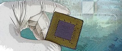
Pushing the Limits in Package Design and Manufacturing
In the areas of both design and manufacturing, the industry is pushing the limits, even in technologies once thought to be mature. Wafer bumping, wire bonding, and surface mount technology, for example, are all very active topics in the research labs and manufacturing lines. On the design side, work continues in areas like system partitioning, materials, and design tool development. With all of this progress, the bridge that spans them – design for manufacturability (DFM) – has become more important than ever.
This year, for its annual industry update, MEPTEC is bringing together packaging experts in these critical areas and others to present detailed technical updates. Don’t miss your chance to get up to speed on today’s most important topics in packaging, all in one place on one day. The opportunity to learn is enhanced with MEPTEC’s unmatched Silicon Valley networking opportunities built into the day.


