
I was again struck by the same epiphany as last year as I escaped the Californian sun to reach the air-conditioned Flash Memory Summit (FMS). The major part of the solid state storage industry depends on NAND Flash. All NAND Flash, whether it be 2-D or 3-D, floating gate or charge trap, depends on a quantum mechanical effect called tunneling or barrier penetration. This effect, discovered in the late 1920’s and applied to silicon devices in the late 1960’s, has been at the heart of NAND Flash program and erase (P/E) since its inception in the late 1980’s. Since the same quantum barrier penetration turns out to form the basis of energy production in the sun, you could say I was escaping the effects of natural tunneling to reach tunneling harnessed by humanity.
What has this got to do with what Schiltron Corporation is up to? In essence, Schiltron’s approach to 3-D memory is designed to wring every ounce of advantage out of Quantum Mechanical (QM) tunneling. Since tunneling has been at the heart of Flash memory for decades, our belief is that the surest path to successful products is to use existing tried-and-trusted mechanisms and materials all in a cost-effective process architecture.
To see why this is important, take a look at Fig. 1 which was part of Western Digital’s Siva Sivaram’s FMS keynote presentation entitled “Storage Class Memory: Learning from 3D NAND”.
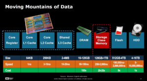
This shows the gap between relatively fast, volatile, expensive, effectively infinite endurance DRAM on one side of the gap and relatively slow, nonvolatile, inexpensive, limited endurance NAND Flash on the other. What is needed is a relatively fast and inexpensive nonvolatile memory with excellent endurance. Differentiation between the storage manufacturers in how they intend to fill this storage class memory (SCM) gap has become clear.
For Western Digital (WD), the path to SCM is 3D ReRAM. The key for them is to combine their 3D NAND architecture with ReRAM. In essence, they intend to swap out the QM tunneling charge storage mechanism for the resistance change in ReRAM material. It appears that their 3D NAND may not have the required speed and endurance required for SCM. WD’s SanDisk arm has a lot of metal oxide ReRAM experience which culminated in a 32 Gbit 2-layer 24nm chip presented at the 2013 ISSCC. The challenge will be its integration into a cost effective BiCS-like architecture and of course control over ReRAM properties.
Samsung announced Z-NAND as their SCM gap filler. No details were given about what Z-NAND actually is except that it “shares the fundamental structure of V-NAND and has a unique circuit design and controller that can maximize performance”. My guess, as others have already stated, is that it is V-NAND SLC. This enhances the endurance from a few thousand to a few tens of thousands of cycles. In essence, it looks like Samsung is staying with QM tunneling charge storage and pushing its endurance by going SLC. Cost effectiveness then comes from using their V-NAND architecture.
We already know that Intel and Micron are going with their 3D XPoint approach for this segment. What it is remains an enigma, but it is certainly not QM tunneling-based charge storage. Their reasons for choosing this path are “up to 1,000 times lower latency and exponentially greater endurance than NAND”. The actual absolute values remain a mystery but, as with WD, it appears that their 3-D NAND may not have the speed and endurance required for SCM. It seems that 100’s of new materials and a lithography-intensive 3-D stacking approach are more attractive than pushing their 3-D NAND solution in the way that Samsung may be doing with theirs. Table 1 is a summary of these SCM approaches. Note the columns for P/E Mechanism, Materials, and Cost Effectiveness.
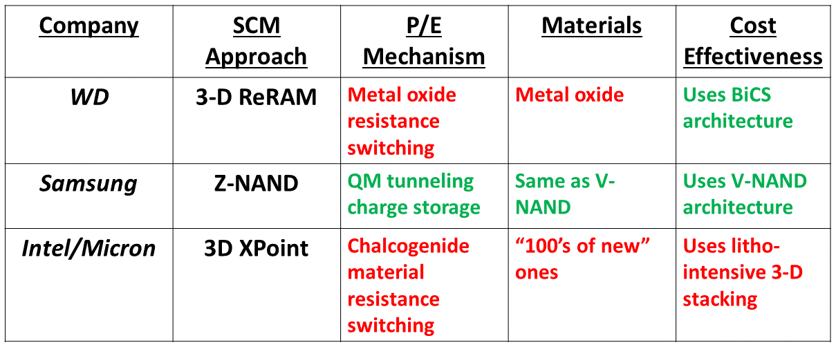
The color coding has the following significance:
- P/E Mechanism:
- Green – mechanism is used in existing semiconductor products and is well understood;
- Red – mechanism is limited to exploratory products or prototypes;
- Materials:
- Green – materials are well known in Fabs and are supported by established tool vendors;
- Red – materials are exploratory and scarce in Fabs;
- Cost Effectiveness:
- Green – low cost per bit (litho-light);
- Red – higher cost per bit (litho-intensive).
This analysis shows that Samsung’s Z-NAND is actually the lowest risk/cost evolutionary approach while 3D XPoint is on the other end of this risk/cost scale. WD’s hybrid approach seems to be a middle path.
How does Schiltron fit into this landscape? Besides a low cost per bit litho-light approach, Schiltron’s materials have been used in fabs for years. But Schiltron’s great advantage lies in its use of QM tunneling in a way that results in orders of magnitude greater endurance than any form of NAND whether it be 2D or 3D, SLC, MLC or TLC.
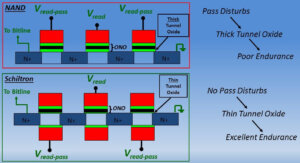
Figure 2 shows a generic cross section of a charge trap (CT) NAND string compared to a Schiltron string. The same considerations apply to any 3D CT NAND. The CT dielectrics are shown as ONO which is shorthand for oxide-nitride-oxide. In the NAND case, electrical communication with any cell requires all other cells to be turned on no matter what their programmed state is. The relatively high read-pass voltage is applied to all the non-selected-for-read cells. This, in turn, requires the tunnel oxide within the CT dielectrics to be made thicker than a single cell would otherwise need to avoid programming these non-selected cells.
In the Schiltron string, the read-pass voltage is applied to independently accessible gates on the opposite side of the thin-film transistor channel. This shields any stored charge from the resultant electric fields. This decouples the ONO optimization from the pass disturbs and allows thin tunnel oxides to be used.
Thin tunnel oxides are in the range of about 17 to 30 Å while 3D NAND tunnel oxide thicknesses are around 50 to 60 Å. This difference is huge on a quantum mechanical scale. Just to give a feel for this, a back-of-the-envelope calculation indicates electron tunneling probability dropping off by ten times for every 1.3 Å added.

The straightforward consideration that thin tunnel oxide ONO is incompatible with NAND Flash was recognized by Samsung in 2006. What was not recognized at the time was the dramatic impact on P/E endurance.
A thin oxide allows direct tunneling of electrons through the oxide and lower overall electric fields in the ONO. These factors were recognized in the 1970’s as being extremely important in original MNOS memories to reliably push endurance beyond 10 billion P/E cycles.
Figure 3 shows Schiltron’s latest data with the threshold voltage window plotted as a function of the number of P/E cycles with the latter taken to 10 million.
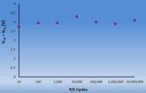
Thin oxide ONO in a thin-film transistor has been shown before to reach at least 1 million P/E cycles with excellent post-cycling retention at 85 C.
Thin oxide ONO has also been at the heart of Cypress nonvolatile memory products for over 10 years with 1 million cycles and 20 years retention at 85 C.
Schiltron’s approach allows such a tried-and-trusted P/E mechanism to be used in an efficient 3-D architecture shown in Figure 4.
And remember that this fruitful area of optimization is completely off limits to the NAND manufacturers because of some fairly simple physics.
In summary, Schiltron combines the evolutionary conservative approach of using existing materials with a cost-effective 3-D architecture. The kicker comes from its ability to use a tried-and-trusted QM tunneling approach, not available to the NAND manufacturers, to reach orders of magnitude improved endurance.
This is the Quantum Mechanical Advantage: A Revolution through Evolution for Storage Class Memory.
~AW