The 2015 3D InCites Awards Judges represent each part of the 2.5D/3D IC ecosystem. This year’s panel includes industry, academia, market research, and R&D, as well as experts in design, test, processes, and manufacturing.
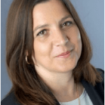 Rozalia Beica, CTO, Yole Développement
Rozalia Beica leads the Advanced Packaging Business Unit and Semiconductor Manufacturing activities within the market research firm, Yole Développement. Beica is an international award (R&D 100) winning scientist with over 60 publications and several patents. For more than 16 years, Rozalia has been involved in the research, application and strategic marketing of Advanced Packaging and 3D IC technologies, with global leading responsibilities at materials (Rohm and Haas), equipment (Semitool, Applied Materials, Lam Research) and device manufacturing (Maxim IC) organizations. She has a Global Executive MBA from IE Business School (Spain), M. Sc. In Management of Technology from KW University (USA) and a B.Sc/M.Sc in Chemical Engineering from Polytechnic University “Traian Vuia” (Romania)
 Surya Bhattacharya, Ph.D. Director, Industry Development, IME
Dr. Surya Bhattacharya directs IME’s 2.5D Integration, Through Si Interposer (TSI) and 3DIC Program. Bhattacharya has over 20 years of experience ranging from 0.8µm to 28nm CMOS. He joined IME from Qualcomm CDMA Technologies, San Diego, CA, where he served as Director of Foundry Engineering, overseeing technology and manufacturing ramps across multiple foundries in Asia and around the world. Previous employment experience includes Principal Foundry Engineer at Broadcom Corporation, Irvine, California, and Senior Manager for CMOS technology at Rockwell Semiconductor Systems, Newport Beach, CA. Bhattacharya holds a Bachelor of Technology degree in Electrical Eng from the Indian Institute of Technology Madras, India, and an MS, and Ph.D Degree in Microelectronics from the University of Texas at Austin, Texas.
 Yann Guillou, Business Development Manager, SEMI Europe Grenoble Office
Yann Guillou is Business Development Manager at SEMI Europe Grenoble Office. His main responsibilities encompass the development of SEMI activities in France & Southern Europe in Semiconductor, PV and Emerging markets and the coordination of SEMI standard activities in Europe. Previously, Yann worked on Advanced Packaging activities within the Back-End Sourcing and CTO & Strategic Planning office of ST-Ericsson. His main interest was 3D integration and TSV. He started his career at CEA-Leti before joining ST Microelectronics and successively worked at ST-NXP Wireless and ST Ericsson.
 Erik Jan Marinissen, Principal Scientist at IMEC
Erik Jan Marinissen focuses his research in the domain of test and debug of integrated circuits. He is a co-author of more than 120 journal and conference papers and a co-inventor of eight granted US and EU patent families. Prior to IMEC, he was with NXP Semiconductors and Philips Research, both in Eindhoven, The Netherlands. He serves on numerous conference committees and editorial boards, and founded such workshops as ‘Diagnostic Services in Network-on-Chips’ (DSNOC) and ’3D Integration’.
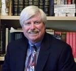 Phil Marcoux, PPM Associates
Phil’s efforts in 2.5D and 3D packaging represent his fourth major new business development. He has been a pioneer in laser trimmed IC devices, surface mount technology, wafer level packaging and now 3D. A common thread in his involvement is multi-chip packaging.
 Herb Reiter, eda2asic
After 20 years in technical and business roles at large semiconductor vendors, Herb Reiter changed to the EDA side to help narrow the gap between EDA tools’ productivity and IC designers’ requirements. Since 2008 Herb has focused his efforts with EDA vendors, large semiconductor companies and IP and design service firms in contributing to the 3D/TSV ecosystem to accelerate market acceptance of this new technology.
 Ira Feldman, Principal Consultant, Feldman Engineering Corp.
Ira Feldman manages and develops unique high technology solutions and business strategies for clients of Feldman Engineering Corp. His goal is to resolve product management and engineering challenges within organizations as well as with their supply chain and customers. His broad knowledge and management experience with high-volume manufacturing of complex technology products is the result of extensive expertise in the semiconductor test and computer test industries.
![Franzon2012crop[1] copy](/wp-content/uploads/Franzon2012crop1-copy-150x150.png) Paul D. Franzon, Alumni Distinguished Professor of ECE. North Carolina State University
Paul D. Franzon, Alumni Distinguished Professor of ECE. North Carolina State University
Paul D. Franzon, Ph.D. is currently a Professor of Electrical and Computer Engineering at North Carolina State University. His current interests center on the technology and design of complex systems incorporating VLSI, MEMS, advanced packaging and nano-electronics. He has also worked at AT&T Bell Laboratories, DSTO Australia, Australia Telecom and three companies he cofounded, PBI Inc., Communica and LightSpin Technologies.
 Peter Ramm, Department Head, Heterogenous Systems Integration, Fraunhofer EMFT
Peter Ramm is responsible for the key competence “Si Processes, Device and 3D Integration”. He received physics and Dr. rer. nat. degrees from the University of Regensburg and subsequently worked for Siemens in the DRAM facility where he was responsible for process integration. In 1988 he joined Fraunhofer IFT in Munich, focusing for more than 25 years on 3D integration technologies. Peter Ramm is author or co-author of over 100 publications and 24 patents.
Larry Smith, Ph.D., Independent Consultant, 3D TSV Technologies, Albany, NY
 Larry Smith previously managed the TSV module in SEMATECH’s 3D Associate Member Technology Development Program. His responsibilities have also included SEMATECH’s 3D Enablement Center, TSV integration and reliability, cost and yield modeling, test vehicle design, and ULK reliability. He has chaired several workshops on critical 3D issues, including Reliability and Manufacturability, Design and Test, Stress Management, and ESD. Prior to joining SEMATECH, he managed the design group for thin-film-on-laminate (XLAM) BGA substrates at Kulicke and Soffa, and programs on multi-chip packaging at MicroModule Systems, Dell Computer, and MCC. Dr. Smith received his B.S. from MIT, his Ph.D. from the University of Illinois, and was a Research Fellow at Harvard University (all in Physics), and developed high speed digital and analog superconductive devices at the Sperry Research Center and the MIT Lincoln Laboratory.
 Paul Werbaneth, 3D and MEMS Industry Journalist, Petaluma CA
Paul Werbaneth writes regularly for 3D InCites on 2.5D/3D IC technology and commercialization. He is a guest editor for IEEE Transactions on Semiconductor Manufacturing, and contributed a chapter on TSV Etching in the book “3D Integration for VLSI Systems”. Paul has worked as a business development manager at EV Group; vice president of marketing and applications at Tegal Corporation; country manager for Tegal Japan Inc.; senior plasma etch process engineer with Hitachi High Technologies; and as a hands-on process sustaining engineer in an Intel wafer fab.
 M. Juergen Wolf, Head of Division Wafer Level System Integration, Fraunhofer IZM-ASSID
M. Juergen Wolf studied electrical engineering and after an industrial carrier, he joined Fraunhofer Institute for Reliability and Microintegration (IZM), Berlin in 1994 working in the field of wafer level packaging and System in Package (SiP). Since 2011 he is head of department Wafer Level System Integration and also responsible for the management of ASSID – “All Silicon System Integration Dresden-ASSID” with its 300 mm 3D Wafer Level Integration line. He is also involved in and leading a number of research projects on national, European and international level.


