On Definitions and Buzzwords Long-time readers of IFTLE know that I’m sensitive about nomenclature and buzzwords. For instance: “nanotechnology” and...
IME – Hybrid Bonding Studies Singapore’s Institute of Microelectronics – IME / AStar – was certainly the most prolific presenter...
The IEDM conference always has a great display of leading-edge technology in the papers, but I always find a great...
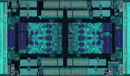
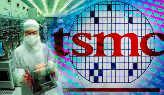
More on TSMC’s SoIC Hybrid Bonding Technology Nikkei Asia announced that TSMC is working with Google and AMD to develop...
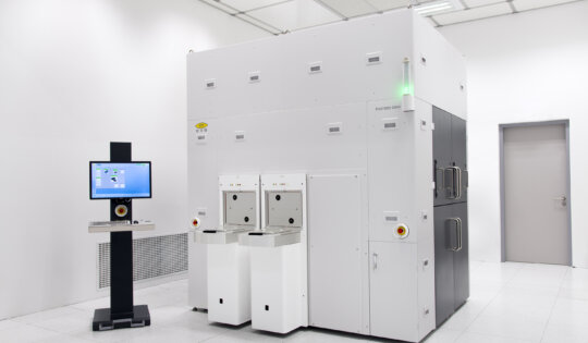
EVG®320 D2W die preparation and activation system provides seamless integration with third-party die bonders; completes EVG’s equipment portfolio for end-to-end...
See that title? That was only part of how I spent last Thursday (December 3). My morning started with the...
EV Group (EVG), a leading supplier of wafer bonding and lithography equipment for the MEMS, nanotechnology and semiconductor markets, today...
I first started covering Ziptronix and its hybrid bonding technology back in 2007 when I was writing Perspectives from the...
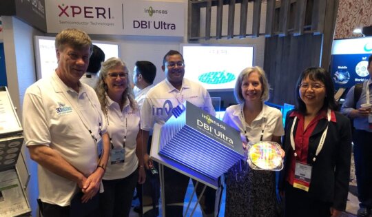
Last year at ECTC 2019, Xperi officially launched DBI Ultra™; the die-to-wafer hybrid bonding version of the highly successful, wafer-to-wafer...
The expansion of hybrid bonding as a process for high-density packaging was the topic of some presentations presented at the...
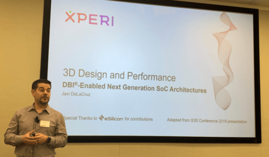
The monthly MEPTEC Luncheons at SEMI in Milpitas focus on microelectronics packaging and test topics. Javier DeLaCruz, Xperi’s VP of...
Requirements for interconnect pitches of 20µm and below is expected to be the norm in the future. Since typical solder...
The Microelectronics Packaging & Test Engineering Council (MEPTEC) held its monthly meeting at SEMI in Milpitas on April 10. Two...
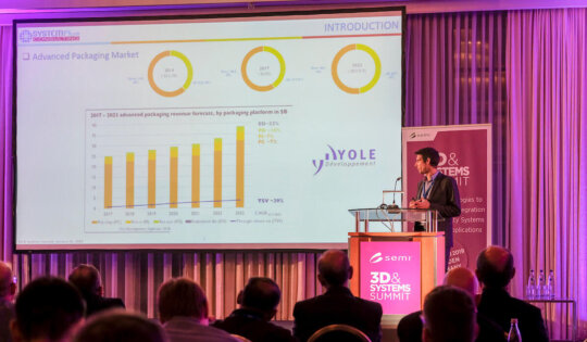
Continuing our look at the 2019 SEMI 3D and Systems summit in Dresden, we look at presentations on advanced packaging...
SAN JOSE, Calif. (August 2, 2018) – Xperi Corporation (Nasdaq: XPER) (“Xperi”) is pleased to announce a partnership with leading...
The special Tuesday session at ECTC 2018 took a look at new methods and applications for assembly technology to accommodate...
Hybrid bonding is quickly becoming recognized as the preferred permanent bonding path for forming high-density interconnects in heterogeneous integration applications,...
2017 saw a clear breakthrough for 3D chip technology in commercial products. Before then, the industry had looked rather...
EV Group (EVG), a leading supplier of wafer bonding and lithography equipment for the MEMS, nanotechnology and semiconductor markets, and...
Every year, I attend most of the events that are focused on 3D integration and related approaches to semiconductor advanced...