


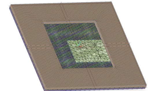
Thermal Simulation of a Packaged GaN MMIC
StratEdge has been designing and manufacturing packages for high-power, high-frequency compound semiconductors since the early 1990s, with much attention focused on gallium arsenide (GaAs) and gallium nitride (GaN). Because of its ability to operate at very high currents and high voltages, gallium nitride GaN is widely used in applications for...

IFTLE 591: TSMC AZ & Samsung get CHIPS Money; IMAPS Hosts 2nd Annual Onshoring Conference
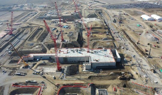
We all knew it was coming….it was just a matter of time until it was announced. The Department of Commerce unveiled its 5th program under the CHIPS and Science Act, this time with TSMC, or more accurately TSMC Arizona Corporation (TSMC-AZ), a subsidiary of Taiwan Semiconductor Manufacturing Company Limited. The...

SEMI Kicks off Year Three of the SCC and Startups for Sustainability
It is popular for mainstream media to publicize different industry’s energy consumption and environmental habits. The semiconductor industry is not immune to this occasional finger-pointing concerning energy consumption, water consumption, and hazardous chemicals that are used to produce the chips that are ubiquitous in our daily lives. Major publications highlight...
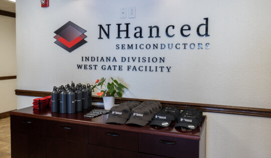
IFTLE 590: The NHanced Semiconductors Roadmap
If you have been following the announcements from Bob Patti and his company, NHanced Semiconductors, it would not be surprising if you were a bit confused about how all these announcements will be coming together. I know IFTLE was, so we approached longtime friend Bob Patti and came up with...
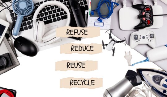
Sustainability 101: Refuse, Reduce, Repair, Refurbish, Rework
The Hierarchy of the Re’s You are probably familiar with the phrase “reduce, reuse, recycle.” You may have heard that it’s best to do things in that order. I suspect that you aren’t aware of starting with Refuse. As a verb, refuse means to say no to something. When individuals...
Five Workflows for Tackling Heterogeneous Integration of Chiplets for 2.5D/3D
Keeping pace with Moore’s law continues to be challenging and is driving the adoption of innovative packaging technologies that support continued system scaling while doing so at lower costs than comparable monolithic devices. These packaging technologies disaggregate what would typically be a homogenous, monolithic device — like an ASIC or...

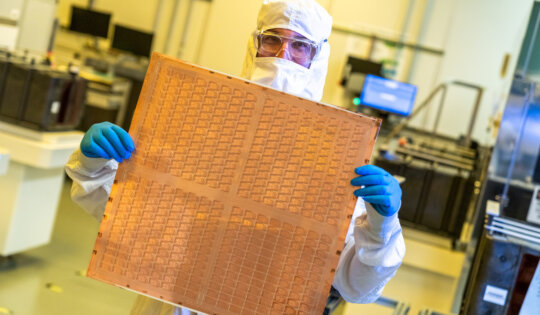
The Role of 200mm Manufacturing in Enabling a $1 Trillion Semiconductor Industry
The global semiconductor industry is growing steadily as integrated circuits (ICs) are now a pervasive part of our everyday lives. Despite recent supply shortages and other challenges, semiconductors are nevertheless projected to become a US$1 trillion industry by 2030, with more than two-thirds of overall growth expected to be driven...
Taking Stock of Global Investments in Semiconductor Manufacturing
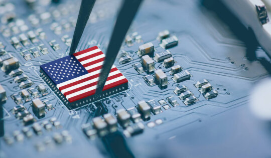
The geopolitical race to take the lead in semiconductors is heating up as global investments in semiconductor manufacturing take hold. Several weeks ago, the Department of Commerce finally made a big US CHIPS Act award, giving Intel $8.5 billion of the allotted 38 billion set to go to semiconductor manufacturing....
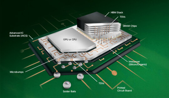
Solving the AI Puzzle
An AI package is like a puzzle made up of individual pieces of different sizes and shapes, each one essential to the final product. Together, these pieces are typically integrated into a 2.5D IC package designed to reduce footprint and maximize bandwidth. A graphic processing unit (GPU) and multiple 3D...
EV Group: More than 40 Years of Growth Fueled by 3D/Heterogeneous Integration
Riding the 3D/Heterogeneous Integration Wave For decades, the ability to achieve the necessary power, performance, area, and cost (PPAC) in semiconductor manufacturing had been largely driven by 2D design rule shrinks enabled through advances in lithography. In recent years, however, the rising costs and complexity associated with 2D shrinks have...
IFTLE 589: Intel Gets CHIPS Act Funding; Raytheon and AMD Partner on Multi-Chip Package
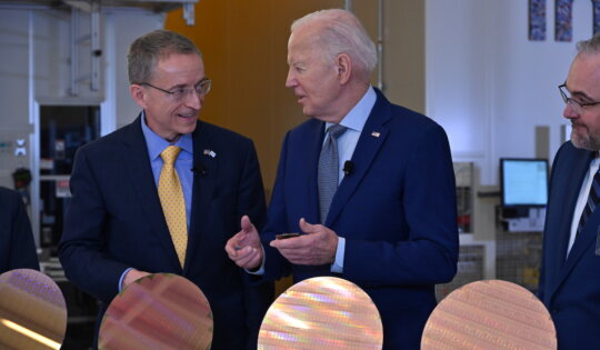
The Department of Commerce (DoC) has announced Intel as the fourth program it will fund under the CHIPS and Science Act CHIPS for America includes the CHIPS Program Office (responsible for manufacturing incentives), and the CHIPS Research and Development Office, (responsible for R&D programs). Both activities sit within the National...
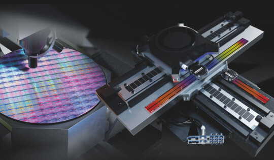
Balancing Precision and Throughput in 3D Structures with Advanced Packaging and Motion Control
The relentless drive in the semiconductor industry to consistently deliver improved performance and power efficiency has traditionally led to increasingly smaller device geometries. However, these tiny footprint dimensions are starting to hit upon a process complexity and are becoming overly expensive to manufacture. Nobody can deny that keeping up with...

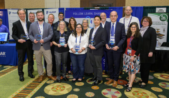
March Member Highlights: Anniversaries, Events, Collaborations, New Products, and More
March buzzed with innovation and collaboration in the semiconductor industry, as key players across the globe joined forces to advance technology, foster education, and address sustainability challenges. From groundbreaking product launches to strategic partnerships and workforce development initiatives, here are the highlights of 3D InCites members’ industry news, events, and...
IFTLE 588: CHIPS NAPMP Materials & Substrates Program
The Creating Helpful Innovations in the Production of Semiconductors (CHIPS) workforce initiatives are shown in Figure 1: The CHIPS vision for success for the National Advanced Packaging Manufacturing Program (NAPMP) is to establish U.S. leadership in advanced packaging and provide the technology needed for packaging manufacturing in the U.S. Ex-IBM...
IMAPS DPC 2024 Makes Advanced Packaging Fun Again!
At last week’s International Microelectronics and Packaging Society’s Device Packaging Conference, (IMAPS DPC 2024) we didn’t need TrendForce to tell us that advanced packaging is the hottest technology in the semiconductor industry. We just needed to look at the record attendance of more than 700 advanced packaging enthusiasts who turned...

Electronics Recycling: There’s Gold in Those Old Electronic Gadgets!
When you replace your PC with an AI-enabled one, will you make sure your old device goes into an electronics recycling program? In November of 2023, I wrote about artificial intelligence (AI) personal computers (PCs) possibly being a growth driver of the 2024 PC and semiconductor growth. Our trusty editor...
IFTLE 587: Intel Glass Core Substrate Update
In late Feb INEMI hosted a Packaging Tech Topic Webinar: Glass Substrates for Advanced Packaging which was presented by Dr. Dilan Seneviratne and Dr. Gang Duan of Intel Corporation. Dilan Seneviratne is a Principal Engineer and Director of Dielectrics and Surface Prep Area within Intel’s Substrate Packaging Technology Development organization....

Driving Into the Future: The Next Phase in Automotive Compute Package Adoption
Automotive compute processors are rapidly adopting advanced process nodes. NXP announced the development of 5nm automotive processors in 2020 [1], Mobileye announced EyeQ Ultra using 5nm technology during CES 2022 [2], and TSMC announced its “Auto Early” 3nm processes in 2023 [3]. In the past, the automotive industry was slow...

Sustainablity 101: Build a Better ESD Bag
When I worked for Advanced Packaging magazine in the early 2000s, we sometimes got pitches from companies that made cardboard boxes or foam cushioning materials. Their spokespeople obviously had not read the magazine or looked beyond the word “packaging” in the title. We ignored those pitches. However, many levels of...

Will the Intel Foundry Model Succeed?
The foundry world has been big news in the past few weeks. TSMC started up the Kumamoto Fab, Japan’s leading-edge semiconductor technology center, partnering with Tenstorrent on RISC-V and chiplets to be manufactured at Rapidus. The biggest non-surprise news flash was the roll-out of Intel’s Foundry Direct Connect, which they...