


Chiplets and 5G were a kind of buy-in to play at the IMAPS 2019 Symposium high-stakes table last week in Boston, MA, but it was heterogeneous integration that took many a pot during the three days of the symposium, particularly when IBM Research held the HI cards.
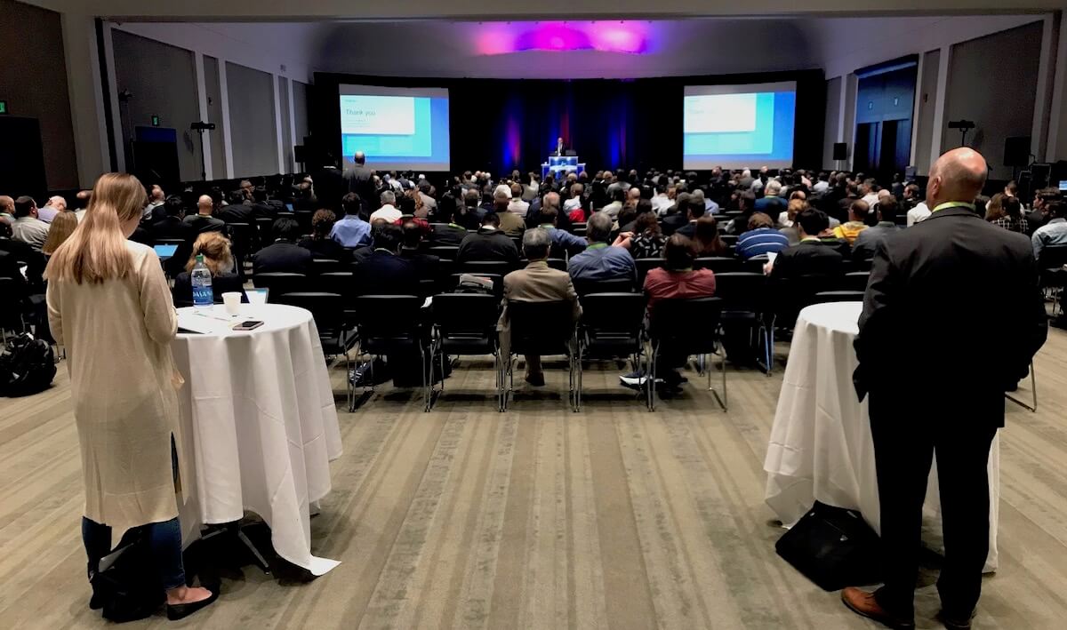
The quick summary from IMAPS about attendance at the Symposium is that “Final registration figures proved that IMAPS 2019 was the industry event to attend this fall, welcoming 918 total attendees – the highest since 2016! Of those attendees, nearly half were drawn from the northeast corridor of the US and 15% were international. More first-time attendees registered for the Symposium than any other in recent memory and nearly 500 different industry organizations were represented.”
The quick summary from me is that IMAPS 2019 was three excellent days of learning, networking, and having fun, while in the presence of the best minds working on semiconductor device packaging today.
All Roads Lead to 5G
Following a day devoted to professional development courses on Monday, September 30, 2019, the IMAPS 2019 program led off on Tuesday the 1st with an opening keynote presentation by Ahmer Syed, Qualcomm, on “Packaging Innovations for 5G Enablement.”
If whatever form of transportation you chose to reach Boston got you to Ahmer’s talk on time then you were luckier than me (I’m looking at you JetBlue 1986 PIT – BOS). The gist of the talk was on the present and future packaging technologies enabling 5G communication, and how “5G brings along the prospect of much higher data speeds, low latency, improved capacity, and potential for new industries.”
All good; “However, the addition of 5G in cell phones poses challenges with additional antennas, exploding number of bands, and added functionality. IC packaging innovations in the form of SiP packaging, antenna beamforming, and new materials are critical to enabling 5G while maintaining a similar phone size, battery life, and thermal performance.”
And right there you have several of the IMAPS 2019 major themes that were expounded on throughout the technical program: SiP packaging; antennas, of the beamforming and/or in-package varieties; and new, 5G-compatible materials. Quite an overture.
Are Chiplets the Stuff of Aristotle?
I managed to connect Thomas Edison with advanced packaging in my most recent blog, a stretch of only a few decades between progenitor and offspring, but Milind Bhagavat, AMD, managed, in his keynote presentation (“Aristotle & Packaging: Making the Products Greater than Sum of their Chiplets”), to connect Aristotle with advanced packaging, which covers a span of about 2,300 years, from the Classical period of Ancient Greece, Aristotle’s era, to this, our age, the Anthropocene.
Dr. Bhagavat told us that the trend in semiconductor design today generally is away from bigger and bigger chips, due to reticle size limits, and because 7nm process technology is hard enough as it is. As a result, there is an opening for chiplets, not necessarily a new idea, but an idea whose time seems to have come. (“It may prove to be more economical to build large systems out of smaller functions, which are separately packaged and interconnected. The availability of large functions, combined with functional design and construction, should allow the manufacturer of large systems to design and construct a considerable variety of equipment both rapidly and economically.” G. Moore, “Cramming more components onto integrated circuits”, Electronics, vol. 38, no. 8, 1965.)
“Nothing in this industry works if there’s no financial impetus,” Dr. Bhagavat reminded us, and his take, regarding advanced packaging of chiplets, is that the technology is both a necessity and that it is a differentiator.
![[err-ad-fallback-title]](http://www.3dincites.com/wp-content/plugins/a3-lazy-load/assets/images/lazy_placeholder.gif)
The success of chiplet schemes will depend on how efficiently they are able to communicate, both chiplet-to-chiplet signals, and signals from the “woven” chiplet fabric (the AMD Infinity Fabric?) to and from the outside world. Milind said that communication occurs over two general kinds of interconnect: near-monolithic, and more-than-monolithic, the former traditional in nature, and the latter enabled by 3D IC technology. Coming up next: exascale processors, chiplet-based, implemented, perhaps, with a third kind of interconnect, optical.
Leave it to Mark Downey, Analog Devices, to voice the pull-quote of the symposium: “When someone in this industry says something’s dead, it’ll still around for 30 years.” (Amen, Mark. Just check out the Intel 8048 microcontrollers I used to make in 1980 – still going strong today.)
Death of Moore’s Law, or Just Stalled Scaling?
And about that stalled scaling … if your ear-to-the-ground has you coming to any conclusions about the pace of semiconductor process node commercial roll-outs today, it’s probably your conclusion that things have slowed considerably. Or just stalled, even as the market for advanced semiconductor-based applications (ADAS, AI, AR) races ahead. Which brings us to “3D Integration for AI Architectures,” an exceptional talk, standing room only, given by Mukta Farooq, 3D Integration Leader for the Artificial Intelligence Center (AIC), IBM Research.
What is the answer to stalled process node scaling? In the AI world, per Dr. Farooq, it’s this: “Cognitive systems are becoming disaggregated.” The means by which they do this is by going from leading-edge process node SoC silicon to architectures based on heterogeneous integration, particularly heterogeneous integration that incorporates 3D IC components.
Mukta stated that “3D is a fundamental pillar for heterogeneous integration AI,” and offered the current generation of Sony CMOS image sensors, comprising three different chips (sensor, logic, memory) created in three different fabrication technologies, stacked using 3D IC packaging, as the ne plus ultra example of what’s being accomplished with commercial 3D IC technology today.
AI needs high bandwidth memory access to be fast and effective, and 3D IC heterointegration of disaggregated components looks like a winner, stalled scaling be darned.
From Pittsburgh, PA, thanks for reading.
~PFW


