


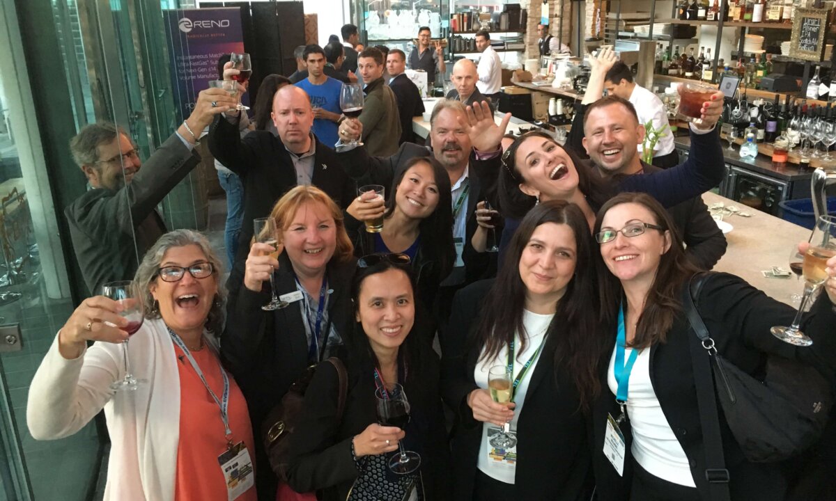
Generally, I avoid reading other journalists’ coverage of events I’ve attended until I’ve had a chance to finish my own coverage. But there it was in my inbox in a recent edition of Semiconductor Packaging News: “Five Takeaways from Semicon” by Semi Engineering’s Mark LePedus. I couldn’t resist. I had to click. I must admit, Mark is more of a hardcore technology journalist than I am, with a more pragmatic lens. I also tend to don my rose-colored “Pollyanna” glasses. So without further ado, in words and pictures, I bring you the brighter side of SEMICON West.
SEMICON West 2017: A Look Back from 3D InCites on Vimeo.
Changing with the Times
David Anderson, the new president of SEMI Americas, reported that SEMICON West 2017 featured 530 companies exhibiting in 1150 booths. 18% of visitors are international, representing 14 countries. The theme: “Smart Starts Here”, was chosen to align with four strategic growth areas: smart automotive, smart manufacturing, smart medical technologies, and the internet of things (IoT). “Smart Starts Here fits with SEMI’s mission and reflects the many opportunities’ across entire semiconductor supply chain, where R&D and manufacturing are vital to the future,” he said.
While, like LePedus said, the show floors seemed smaller and less populated than in the past, I attributed that to the construction happening at Moscone South, and the convergence of front and back-end exhibitors combined into West and North. As far as fewer press events and briefings, it seems that those have fallen off due to reduced press corps attendance. My docket was as full as ever, and I had to miss two networking events I usually attend because the 3D InCites Awards were held the same evening. Additionally, the SOITEC press luncheon was a welcome addition – the likes of which I hadn’t seen in a few years.
Business is Booming
According to Ajit Minocha, the new president of SEMI Global, we can expect 2017 to be the best year ever, with the industry pushing towards all-time records: A $1.6T electronics industry, with $400B revenue in semiconductors alone. Much of this will be fueled by China’s investment in semiconductor manufacturing, as evidenced by an unheard of 24 fabs popping up since last year. In fact, SEMI’s Dan Tracy predicts China will lead the world in 200mm fab expansion and be the number two spending region in 2018.
Tracy cited across-the-board growth indicators such as increased data and technology transformation. Smartphones are back on the radar, he said, and it’s been a good year for the automotive, and 3D NAND continues to drive growth in the memory markets. Tracy also said that over $10B is being spent on equipment and materials in North America and that growth is expected to continue thanks to growth at leading edge fabs like Intel and Micron. Check out Paul Werbaneth’s post for more insights from SEMION West sessions.
And from The Suppliers: Revisiting Laser Debond
What’s old is new again. I’m not talking about bell bottoms and tie dye. In this case, it’s laser debonding for temporary bond/debond processes, which was developed more than 10 years ago and never really took off. Unlike these early approaches that used an infrared (IR) laser source to ash the temporary bonding material followed by a peel step, EV Group’s new laser debonding system uses a solid-state ultraviolet (UV) laser that chemically breaks the molecular bonds of the polymer, which can then be cleaned off the device wafer with a simple solvent without causing mechanical stress to the chip, thereby improving yield and ensuring reliability, said Markus Wimplinger, EV Group. Additionally, the polymers used with IR technology were transparent. An IR laser can damage the device through the slightest pinhole. Alternatively, UV lasers can be absorbed without damaging the device.
“This is a strong product that is compatible with a range of materials on the market,” noted Wimplinger. “Our open platform opens up the materials space and allows customers to work with their suppliers to choose the right material for the application.”
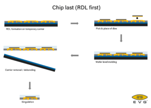
Development of this system was motivated by fan-out wafer level packaging (FOWLP) technologies, and particularly RDL-first (chips last) approaches (Figure 1). Wimplinger explained that this is because RDL first involves the build-up of high-density RDL on top of bonding layers, and require a glass carrier with a thin adhesive that can be debonded using low force. And because it requires low temperatures, UV laser debond is ideal for temperature sensitive process steps. Beyond FOWLP, its application space includes memory, interposer, logic, MEMS, and more.
“Packaging houses needed a very versatile temporary bonding solution that requires them to think less about the integrated process flow,” explained Wimplinger. “This can be used for most situations in the silicon world that use glass carriers. The only limitation is when Si carriers are required. In that case, other technology choices, such as mechanical debond, is a better solution.”

Fan-Out Calls for New Debond Materials
The industry called and once again, Brewer Science is delivering, by adding yet another generation to its already robust portfolio of temporary bond/debond solutions. It’s no wonder they brought home a 3D InCites Supplier of the Year Award this year.
According to Ram Trichur, Brewer Science, thanks to its high mechanical and thermal stability, Gen 4 addresses novel challenges associated with FOWLP die first approaches, such as wafer warp, and die shift. As Trichur explains it, RDL layers are built on the backside of the wafer require 10 hours of high-temperature processing, during which the wafer “wants to peel away”. Gen4 provides a thermoplastic layer on the device wafer side with a curable layer on the carrier wafer side for improved adhesion to make the wafer rigid and thermally stable through FOWLP processes.
This room temperature bonding material, which is stable up to 350°C, is compatible with both laser and mechanical debond in both wafer and panel formats, noted Trichur.
On the Metrology Front
I caught up with Lars Markwort, director of business development for FRT GmbH, suppliers of 3D surface metrology systems, to learn a bit more about the company’s unique approach to metrology. While FRT wasn’t showcasing any new products, I realized that while I talk to CEO Thomas Fries often at the European MEMS and 3D Summits, we’ve never actually had a formal briefing to discuss FRTs product offering in detail.
FRT’s core technology combines multiple optical sensors and proprietary software to perform 3D metrology on a multitude of surfaces in a diverse range of industries including semiconductor, microelectronics, optical, photovoltaics, automotive and more. Market leaders in MEMS metrology solutions, according to director of business development, Lars Markwort, FRT has its eyes firmly on the advanced packaging markets.
Employing such capabilities as white light interferometry and atomic force microscopy, and confocal chromatic sensing, FRT systems offer a wide range of point, field-of-view, and film thickness optical sensors that can be combined in 35 different configurations with up to seven sensors on one platform. Software defines the measurements being taken and determines which sensor will be used. A 3 x 3-inch exposure field is used and stitched together to offer a scalable solution. “This way, we can extract richer 3D data from the whole wafer that allows for metrology that can also be used for inspection,” said Markwort. For example, in the case of determining coplanarity of Cu pillars, the height and shape measurements also reveal if there is erosion around the pillars, or if there are any missing. The company is targeting 3D through silicon vias (TSVs) with dual sensor configurations to measure thin wafers and TSV total thickness variation, as well as edge inspection, and overlay inspection in FOWLP. Additionally, FRT is seeing an increase in interest for front-end metrology for advanced lithography, CMP, and 3D NAND, all of which have wafer surface topography that needs to be monitored. All of this is adding up to increased engagements overall.
And that’s not all…
Wondering how the shift in from dimensional scaling to heterogeneous integration is impacting the industry? Read my two-part series here. And for more highlights of SEMICON West, read my blog post on the Kiterocket web site. ~ FvT


