Jun 11, 2013 · By Francoise von Trapp · 3D In-Depth
Product Description Tessent Memory BIST (built-in self-test) allows you to test and diagnose failures in memory die and in the through-silicon-via (TSV) connections between the memory and logic die within a stacked package. This solution supports any memory stacking configurations without any change to the test infrastructure Testimonial The Tessent...Jun 06, 2013 · By Francoise von Trapp · 3D Event Coverage
At ECTC 2013, Dow Corning Corporation (DCC) introduced its solution to the temporary bond/debond conundrum. During the materials and process session, Ranjith John, materials development & integration engineer at Dow Corning, presented a paper titled Low Cost, Room Temperature Debondable Spin on Temporary Bonding Solution: A Key Enabler for 2.5D/3D...Jun 05, 2013 · By Francoise von Trapp · 3D Event Coverage
A few weeks ago I spoke with SPTS’s David Butler, after he participated in the SEMICON Singapore 3D IC panel. We talked a lot about the importance of wafer planarity for performing backside processes like TSV reveal. Butler commented that regardless of a tool’s calibrated precision, its only as good...Jun 04, 2013 · By Francoise von Trapp · 3D Event Coverage
This year’s 3D InCites coverage of ECTC 2013 features a series of interviews with suppliers to the 2.5D and 3D IC market. I spoke with a number of exhibiting and attending companies who had progress reports on their tools, processes and materials aimed at leaping over the remaining hurdles. The...Apr 10, 2013 · By Francoise von Trapp · 3D In-Depth
Naysayers be damned! Full commercialization for 3D ICs in smartphones may be a few years out, but that doesn’t dampen the spirits of the truly devoted, who latch on to every forward step as a monumental accomplishment. This week, progress appears to be taking off for 2.5D products, and the...Apr 08, 2013 · By Francoise von Trapp · 3D In-Depth
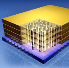
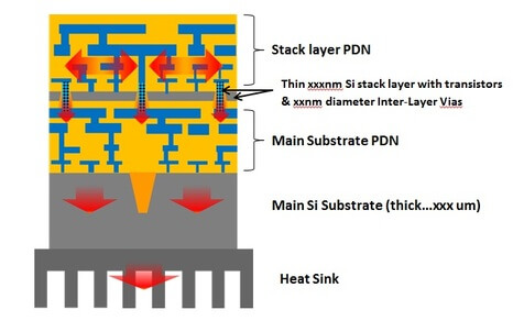
3D ICs have clearly caught the eye of the military and aerospace electronics industries. I came across two separate announcements – one from Georgia Institute of Technology and one from IBM Microelectronics – that each had been awarded DARPA grants to work on chip-level cooling technologies as part of the...Apr 04, 2013 · By Francoise von Trapp · 3D In-Depth
Not long after posting 3D IC Reality Check on Tuesday, I discovered that I missed one. If you haven’t read the post by SemiMD’s Mark Lepedus, Industry Inches Towards 3D Chips you should. While its got some similar information about recent announcements from GlobalFoundries as was in Rick Merritt’s post in EETIMES, it has...Apr 03, 2013 · By Francoise von Trapp · 3D In-Depth
At the BiTS Workshop 2013, the talk show segment, Talking Points, examined the concept of Interconnectology and how adopting new terminology can inspire a paradigm shift in the design and development of next-generation interconnect technologies, thereby impacting the semiconductor device manufacturing value chain. Hosted by Françoise von Trapp, 3D InCites,...Feb 22, 2013 · By Francoise von Trapp · 3D Event Coverage
Has it really been a month since the European 3D TSV Summit? This inaugural event certainly caused a buzz in the blogosphere! In addition to all my coverage after having attended the event, Phil Garrou has been slogging his way thorough the proceedings to provide an in-depth review on Insights...Feb 04, 2013 · By Francoise von Trapp · 3D Event Coverage
It had been awhile since I heard from the folks at Alchimer about the progress of electrografting (eG), its “all wet” nanometric film deposition processes. For a while, it seemed like there were exciting things to report every few months, and then POOF – All went dark. So I was...Jan 15, 2013 · By Francoise von Trapp · 3D In-Depth
No sooner did I post last week’s curation of predictions for the semiconductor industry, and particularly for 3D ICs, than several more popped up online. I suspect this type of thing to continue for the next few weeks, and I will try and continue to cherry-pick the ones that made...Jan 08, 2013 · By Francoise von Trapp · 3D In-Depth
It’s that time of year again when various electronics trade publications invite industry executives to peer into their crystal balls and make their predictions for the coming year. I’ve been perusing through everything from overall industry forecasts by market analysts to suppliers eager to promote their core competencies for 3D...Jan 04, 2013 · By Francoise von Trapp · 3D In-Depth
I don’t know about you, but I always find that amidst the holiday hubbub, the really important stuff gets shoved aside and falls through the cracks. Just in case you missed them, here are some good 3D related posts that may have been lost in the December race to “get...Dec 21, 2012 · By Francoise von Trapp · 3D Event Coverage
It’s too bad SUSS MicroTec’s Wilfried Bair was one of the last presenters on Friday at 3D Architecures for Systems in Packaging Symposium (3DASIP), Dec. 14, 2012, because more people should have been present to hear what he had to say. While most presenters focused on successes and future work...Dec 13, 2012 · By Francoise von Trapp · 3D In-Depth
Yesterday at the pre-conference symposium for 3D Architectures for Semiconductor Integration and Packaging (3D ASIP), I was fortunate to get an up close and personal tutorial preview by David Wang, CEO of ACM Research, on the tool manufacturer’s latest process solution for two critical points in the TSV fabrication process. The...Dec 10, 2012 · By Francoise von Trapp · 3D In-Depth
There are a couple of notable updates circulating this week involving companies in the 3D space. The first I saw was news from Sony that it has introduced its next-generation CMOS Image sensor they claim is “ the industry’s smallest, CMOS image sensor and camera system”. The image sensor is...Nov 28, 2012 · By Francoise von Trapp · 3D In-Depth
The first European 3D TSV Summit (January 22-23, 2013) hasn’t even happened yet, and already its intended message is becoming clear: Europe is ready to tackle those remaining issues and lead the world down the home stretch. It makes sense, since Europe’s R&D centers (imec, CEA Leti, Fraunhofer IZM) has...Nov 20, 2012 · By Francoise von Trapp · 3D In-Depth
Multi-Die Integration Provides Multifaceted Solutions By Francoise von Trapp, 3D InCites This year’s Roadmaps for Multi-Die Integration Symposium, hosted by MEPTEC on November 14, 2012 at the Biltmore Hotel in Santa Clara, CA, offered some interesting and different perspectives than the garden-variety 2.5D and 3D IC conferences of late. While...Nov 14, 2012 · By Francoise von Trapp · 3D In-Depth
Last week (November 6) STATS ChipPAC issued a press release announcing that its advanced eWLB provides a platform for 2.5D and 3D technologies. In search of further information about this, I found a feature article recently published in Solid State Technology that explained how eWLB can be leveraged for 2.5D and...Nov 12, 2012 · By Francoise von Trapp · 3D In-Depth
The latest digital issues of Chip Scale Review and iMicronews’ 3D Packaging magazines hit the virtual “stands” last week, and perhaps in honor if the 3D ASIP Conference that gets underway later this week, there are some hot new 3D technologies being featured. But first, to bring everyone up to...