Jul 15, 2014 · By Francoise von Trapp · 3D Event Coverage
The winds of change are blowing in the semiconductor industry. And while some cling tightly to the way things have always been, it’s becoming more apparent that for those who can adapt, there are a multitude of opportunities, and for those who think it can stay the same, it will...Jul 11, 2014 · By Francoise von Trapp · 3D Event Coverage
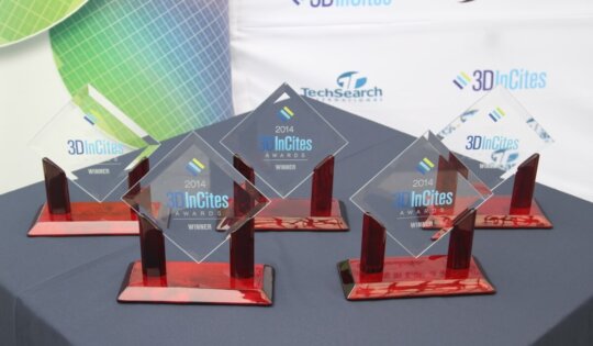
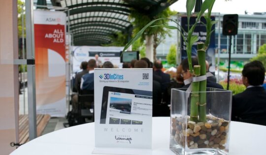
For the second consecutive year, a sizable group of 3D integration enthusiasts gathered at the Impress Lounge to honor the innovators in 2.5D and 3D technologies at the 2014 3D InCites Awards Breakfast. The program included a thought-provoking keynote by Bryan Black, Senior Fellow at AMD, as well as brief...Jul 11, 2014 · By Francoise von Trapp · 3D In-Depth
With the continued innovations in packaging technologies and 2.5D interposers pushing 3D ICs further out from one end, and 16/14nm nodes already qualified without TSVs, making us wait until 10nm, are 3D ICs suddenly getting the squeeze from both sides? That’s one theory I took away from all the conversations...Jul 07, 2014 · By Andrew Walker · Blogs
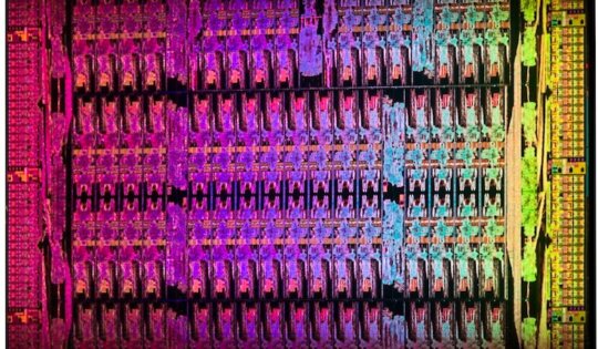
Samsung’s introduction of its 3D NAND Flash SSD 850 Pro has led to the inevitable hullabaloo. Amid all the fuss, it hasn’t taken long for someone to publish the actual die size. This of course is the golden nugget of information that lays the foundation for any cost analysis. Figure 1 shows...Jul 04, 2014 · By Francoise von Trapp · Blogs
The judge’s votes are in and the online poll is closed, and I’m not telling you who won the 2014 3D InCites Reader’s Choice Award. We are saving that, and the announcements of the judges’ picks for this year’s official 3D InCites Awards until the breakfast ceremony on Thursday, July...Jul 01, 2014 · By Francoise von Trapp · Blogs
I don’t know why it still surprises me to read conflicting reports on the progress of 3D TSVs. But I think Ron Huemoeller, Amkor, finally hit on it in his closing remarks during today’s webcast, “TSV Packaging at the Tipping Point”, moderated by Pete Singer, Solid StateTechnology/Extension Media. Huemoeller’s presentation and...Jun 27, 2014 · By Bill Martin · Resource Library
Microelectronic products all have mechanical, thermal and electrical properties that degrade until the device is permanently damaged. Path finding adds value to an end-product by pre-determining where the breaking points are, and if or how they can be enlarged. For decades, product designers have used various methods of path finding...Jun 27, 2014 · By Francoise von Trapp · Resource Library
Jun 26, 2014 · By Bill Martin · Resource Library
2.5D/3D packaging technologies are revitalizing creativity in high technology products. We thought we knew what faster, better, lighter and smaller meant. 2.5D/3D packaging can revolutionize what we thought possible but it will require augmenting our current methods and tools. One key methodology to add would be Path Finding. Path Finding can...Jun 26, 2014 · By Andrew Walker · 3D Event Coverage
Imagine this: aquamarine tints of the Pacific washing sandy Hawaiian beaches amid the balmy breeze and only yards away, several 3D NAND papers being presented at the recent VLSI Symposium in Honolulu. Idyllic! I counted five papers in total associated with various forms of 3D NAND. The protagonists were: SK...Jun 25, 2014 · By Francoise von Trapp · Blogs
Somehow in all my preparations for the 2014 3D InCites Awards and planning the schedule for SEMICON West this week, a significant piece of news slipped right by usually alert 3D radar for TWO WHOLE DAYS! On Tuesday, Micron issued a press release announcing a collaboration with Intel to deliver an...Jun 24, 2014 · By Francoise von Trapp · 3D Event Coverage
I can’t believe it’s already been a year since I last posted my annual guide to 3D at SEMICON West. One thing I’ve noticed in scanning the “regulars” (SEMI and SEMI partner events) is that all the agendas are much less focused on 3D integration developments. I think there are...Jun 23, 2014 · By Francoise von Trapp · 3D Event Coverage
The nominations are officially closed for the 2014 3D InCites Awards; and now comes the fun part. This year, while the industry expert judges will determine the winners of each individual category; one Reader’s Choice Award will be decided by you; the registered members of the 3D InCites Community through an Online...Jun 23, 2014 · By Francoise von Trapp · 3D In-Depth
CIRCL CV310i module is an advanced Wafer Edge inspection, metrology and profiling system tailored for Advanced Wafer Level Packaging. Simultaneous wafer edge inspection and metrology enables comprehensive data collection from all zones comprising the wafer’s edge: top and bottom near-edge; top and bottom bevel; and apex. Testimonial Some of the...Jun 20, 2014 · By Francoise von Trapp · 3D In-Depth
SSEC’s wet TSV reveal process achieves -/+ 0.7% Si thickness uniformity under the appropriate post grinding conditions with fast throughput. The two-step process starts with a spin etch for a smooth, fast etch at 10µm/min. The etch is stopped 2µm above the TSVs and then finishes with a selective etch...Jun 19, 2014 · By Francoise von Trapp · 3D In-Depth
Akrion Systems’ vacuum prime and drying technology enables the use of a wet immersion method to introduce liquid chemicals or rinse water throughout the entire HAR feature prior to the oxide etching step. Pulling a vacuum below the saturated vapor pressure of water, draws liquid into the entire feature, enabling...Jun 18, 2014 · By Francoise von Trapp · 3D In-Depth
Manufacturing of 3D IC heterogeneous integrated modules for the electronics of a leadless pacemaker in a very small volume has been realized. Manufacturing of 3D IC modules using the described process is ready for medium volume production. Testimonial All the electronics of a leadless pacemaker has been integrated into a...Jun 17, 2014 · By Francoise von Trapp · 3D In-Depth
SETNA, in conjunction with Research Triangle Institute (RTI), has developed a binary alloy (Silver-to-Indium) bonding system for 3D IC assembly that can be compression-bonded at room temperature. Following 3D IC chip stacking, the Ag-In structure is annealed in the solid-state (no melting) to form an Ag₂In interconnect which is stable...Jun 11, 2014 · By Francoise von Trapp · Devices
Schiltron 3D Flash replaces 2D-NAND. It uses a unique architecture solving key challenges associated with other 3D-NAND approaches: scalable; no vanishing string currents; uses existing Fab infrastructure and materials; uses existing design approaches for program and erase; endurance of over a million cycles; post-cycling retention of more than 10 years...Jun 11, 2014 · By Francoise von Trapp · 3D Event Coverage
While most of the research institutes in the US and Asia have been focused on commercializing 3D integration technologies for mass markets such as mobile devices and consumer electronics, one US-based research institute has followed a different path more similar to that of the European research centers; focusing its 3D...