


More Spoor: Heterointegration in the 2015 Analog, MEMS and Sensor Startups to Watch, Part 2
In Part 1 of this series I drew your attention to what Peter Clarke, writing in EETimes on 02 January 2015, called the “15-in-15: Analog, MEMS and sensor startups to watch in 2015.” What would we find if we were to look for signs of heterointegration in this particular gathering,...

Measuring The Invisible: An Update on X-ray Metrology
One year ago, I visited Nordson DAGE at its R&D center in Colchester, to learn about the company’s latest foray into X-ray metrology at the production level with the launch of the XM8000. Rather than just using X-ray for inspection, this tool also analyzes the data to allow for full...
Notes from the FOA Packaging and Test Group
The Packaging and Test Group of the Fab Owners Association, (Cupertino, CA) held its first official meeting on February 4th. This was just one of the meetings held as part of the third annual FOA Collaborative Forum in Santa Clara, CA. The fourteen inaugural FOA packaging and test group (FOA-PT) members heard...

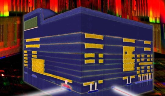
Advances in Heterogeneous Integration Through Wafer Bonding
Emerging “More than Moore” and photonic applications benefit tremendously from the close integration of compound semiconductor materials. Recently, many of the improvements in device performance achieved within the semiconductor industry are a result of innovation and material research rather than traditional downscaling of design features. One of the major new...

Samsung’s V-NAND Flash at the 2015 ISSCC –The Only Way Left is Up
Samsung continued their 3D NAND march with an impressive presentation at the 2015 IEEE International Solid-State Circuits Conference (ISSCC) in San Francisco on February 24th. Their presentation, “A 128Gb 3b/cell V-NAND Flash Memory with 1Gb/s I/O Rate”, listed only 34 authors this time compared to 46 last year. Remember that Samsung...

Addressing Emerging Technology Start-up Dilemmas
We see it all the time, someone has a great idea of how to implement emerging technologies, such as interposer integration, 3D IC, or even high density interconnect (HDI) printed circuit boards, (PCBs) and invests lots of money to develop complex products, only to fail because they chose the wrong...
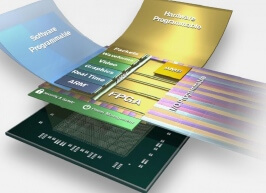
Xilinx Ultrascale+: 3D on Steroids
Ever since 3D transistors (aka FinFETS or Intel’s Tri Gate) 3D NAND, and monolithic 3D IC processes joined the family of 3D integration technology possibilities, we’ve been careful to define them separately on 3D InCites. Some people have wondered if one will displace the other, or if these technologies would...

RIP ITRS V1.0: 1992-2015
Prior to 1992, the high technology industry was ‘immature’. Each supply chain vendor (equipment, materials) would accumulate input from their customers that defined product roadmaps. Vendors cared little about accepting or supplying work-in-progress (WIP) to other vendors’ products. But it became obvious to many that unless they were coordinated, sales potential...

Heterogeneous Integration Spoor In MEMS and Sensor Start-ups
The distinguished journalist Peter Clarke, writing in EETimes on 02 January 2015, identified what he called the “15-in-15: Analog, MEMS and sensor start-ups to watch in 2015.” What better place to shine the heterogeneous integration spotlight than here, I thought, when I read the piece in January – as Peter...

Can Path Finding be used in the Production Environment?
In previous posts, I have discussed various scenarios when Path Finding can be used. All were focused on the early design process: implementation guidelines, robust design and process centering. But what if you have a design in production and ‘something’ happens; like a process is no longer available; a component...

DesignCon 2015: Blasting Through Walls with Holistic Planning
DesignCon’s 2015‘s tag-line “where the chip meets the board”, was a very appropriate message, and summarized in a few words a major trend in our semiconductor- and electronic systems industry: The increasing need for holistic planning as well as modeling of building blocks, not only for better up- and down-stream...

Riding Out on a Horse and in on a Goat: 3D IC Predictions for MEMS
The Lunar New Year is soon upon us, and we will be celebrating the Year of the Goat with firecrackers, red packets (I hope!), and the evening parade in San Francisco on 07 March 2015. The goat is a sturdy animal whose praises are often undersung. Undersung – that sounds...

Advanced Packaging Challenges and Opportunities for 2015
Our industry is seeing greater diversification in manufacturing processes than it has since its earliest days. In the front-end numerous new materials, architectures, and processes are under development to enable the continuing march toward smaller device sizes. In the back-end, and many places in between, advanced packaging processes and 3D...
Silicon Photonics and 2.5D Interposer Design
Historically, we all took Moore’s Law for granted. With each new node, we could expect to see faster-performing devices, smaller design footprints and, ultimately, lower design costs. Nowadays these benefits are not clearly achievable for all designers. At the latest advanced technology nodes, we may be able to see faster...

Micro vs. Macro 3D IC Cost Analysis: Can we learn from the mid 1980’s?
Amy Palesko from SavanSys Solutions wrote an excellent 3D IC cost analysis article (The Cost of 3D ICs) on 3D InCites that focused on the manufacturing cost of TSV enabled devices. No question that these costs are important and will follow a classical manufacturing learning curve. But the real story...

Realistic Expectations for 3D IC Products in 2015
In an era where people expect instant everything, the development of the market for 3D ICs with TSVs has not met many expectations. But for those who really understand how long it takes to bring a new technology to maturity, it should be no surprise. It has taken memory companies...
Executive Viewpoint: An Interposer Integration and 3D IC Success Story
While the rest of the industry anticipates the coming of 3D ICs, and along with it the long anticipated return on investment that goes with it, one small Silicon Valley fabless has been chugging along, already reaping the benefits of interposer integration and 3D IC technologies. I first heard Farhang...

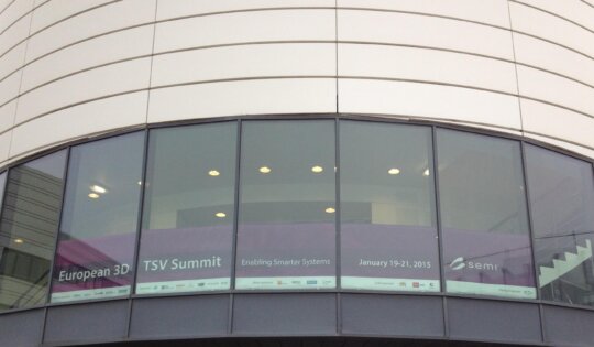
The Discussions Continue at the European 3D TSV Summit
At last week’s third edition of the European 3D TSV Summit, over 250 attendees from 22 countries gathered at Minatec Campus in Grenoble, France to talk about how 3D enables smarter systems. The discussions seemed to picked right up from where we left off at the 3DASIP Conference in December...

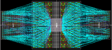
Technology Options and Their Influence on Routing for Interposer-based Memory Processor Integration
Currently in advanced integration, mainly stacked solutions (Figure 1b) are considered due to their attractive compactness. But if the ASIC or the processor is a high-performance circuit, there are problems with the thermal budget of the stacked solution. This is because the valid temperature range of the memory is limited....
Predicting the 3D Integration Market is Tricky Business
Ask any market researcher or business development executive at a major semiconductor manufacturing company; predicting exactly when the 3D integration market is going to take hold and fly is a tricky business, because there are so many elements to consider. During this year’s European 3D TSV Summit pre-conference market briefing,...