


How Will Future Capex Spending Affect Semiconductor Suppliers?
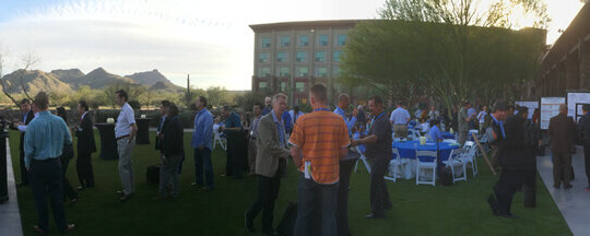
At the recent Arizona SEMI Breakfast Forum, held April 17, 2015, semiconductor suppliers gathered at the Mother Ship (aka Intel) in Ocotillo, AZ, to hear information that could affect their sales of tools and materials, based on the expectations of industry capacity expansion over the coming years. As the theme for the...
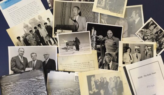
A Trip Down Silicon Valley’s Memory Lane with Bill Hugle
Inspired by all the recent attention for the 50th anniversary of Moore’s Law and SEMI’s cool new Infographic series, which reflects the industry’s role in “Making Small Things Makes Big Things Possible,” my colleague and Impress Labs managing partner, Martijn Pierik, took me on a trip down Silicon Valley Memory...

Goofus and Gallant and the Internet of Things
If you grew up before about the mid 1980’s, you likely remember the magazine, Highlights for Children (now an online publication, Highlights for Kids) and within that magazine you likely recall a cartoon strip regular feature called Goofus and Gallant. The basic premise is that it features two contrasting boys, Goofus and Gallant....
Executive Viewpoint: Inside a Multi-Project Wafer Program for 3D Integration
Multi-project wafer (MPW) programs have long been considered an economical way to integrate different IC designs from various teams to produce IC design prototypes and low volumes. Because IC fabrication costs are extremely high, it makes sense to share mask and wafer resources in this way. MPWs were historically used...
TSMC 2015 Technology Symposium Highlights Plans for the Coming Year
Last Tuesday, April 7, was another important day for Silicon Valley. TSMC 2015 Technology Symposium celebrated 21 years of holding this annual event to update TSMC’s loyal customers and win new ones. Rick Cassidy, President TSMC North America, opened the symposium with a long list of impressive numbers about TSMC and put them into...

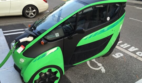
Will the Internet of Things Deliver on its Promise?
“Firsts are good but lasts are better. The Internet of Everything (IoE) is ushering in many firsts but its legacy will be measured in the lasts it creates: the last blackout, the last product recall, the last traffic jam, the last missed delivery…” ~ Cisco The promise the Internet of...

Is Moore’s Law a Ceiling, Or Is It a Floor? More Notes From CS International 2015
Chris Mack, “Gentleman Scientist,” published an excellent piece on March 30, 2015 in IEEE Spectrum on “The Multiple Lives of Moore’s Law – Why Gordon Moore’s grand prediction has endured for 50 years.” (Hint: “hard work, human ingenuity, and the incentives of a free market.”) Moore’s Law has several flavors...
Addressing 3D IC Assembly Challenges at IMAPS DPC 2015
While we wait in the 3D IC holding pattern for products to go into high volume, processes continue to be tweaked and optimized to address the remaining 3D IC assembly challenges. At IMAPS DPC 2015, a number of presentations focused on some of these incremental advancements. Here, we checked in with...

How to Ensure Quality and Reliability in 3D IC stacks
A major concern in 3D IC designs is ensuring reliability and quality. Specifically, there is a growing need for design verification flows that can determine the cross-layer implications of the stresses caused by through silicon vias (TSVs) and chip-package interaction (CPI) induced mechanical stresses. Because 3D IC stacks have limited...

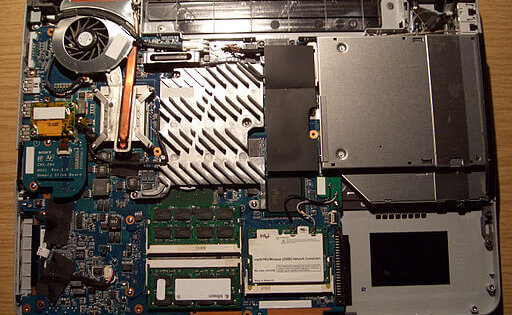
SEMI-THERM 2015: Thermal Innovations that Make the World’s Technology Cool
From March 16-20 the annual SEMI-THERM Conference (SEMI-THERM 2015) in San Jose gave me the opportunity to meet many assembly, materials, and thermal management experts. I also learned a lot about how IC packages and PCBs protect and cool single- and multi-die ICs. Both contribute significantly to cost, performance, and reliability...

Flying Many Flags: Heterogeneous Integration at CS International 2015
The fifth annual CS International Conference, 2015 edition, was held in Frankfurt, Germany, March 11-12, 2015. Very conveniently located in the Sheraton Frankfurt Airport Hotel & Conference Center, just steps away from where I deplaned in Frankfurt after my flight from Dulles. Over the course of its 2 days, CS International 2015,...

DATE 2015 demonstrates Europe’s commitment to Semiconductors, Part 2
Continuing from Part 1: On Thursday morning I really enjoyed the Monolithic 3D session. Francoise already reported about it, so I can be brief and focus on the most advanced program presented, the CEA Leti CoolCube™ . Olivier Billoint showed and explained how Leti, in cooperation with an EDA partner, is...

IMAPS DPC 2015: Has 3D IC Hit a Holding Pattern?
From the perspective of 3D integration and its march towards commercialization, there was not much new being presented at the 2015 IMAPS Device Packaging Conference and the Global Business Council (IMAPS DPC 2015) held concurrently in Fountain Hills, AZ, (March 16-19); at least not since the European 3D TSV Summit 2015, or 3D...
CoolCube™: A True 3DVLSI Alternative to Scaling
Stacking transistors on top of each other sequentially in the same front-end process flow is a concept that has been imagined to provide the semiconductor community with an alternative to the traditional scaling paradigm challenged by technical and cost roadblocks. LETI Advanced CMOS Laboratory introduced CoolCube™, a low-temperature process flow that provides...
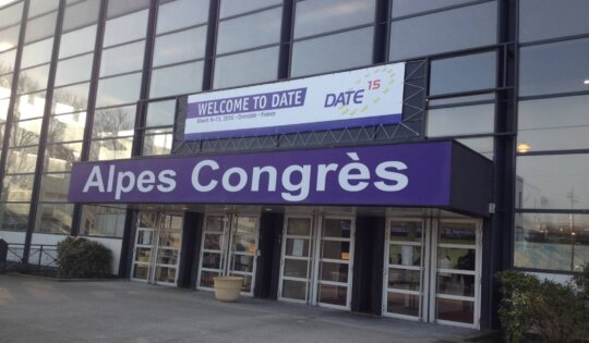
DATE 2015 demonstrates Europe’s commitment to Semiconductors
Full disclosure: I spent the first half of my life in Europe. I was born and raised in Austria, and earned my engineering and business degrees at government funded schools there. I worked more than 12 years in technical and business roles in Munich, covering all of Western Europe. If...

Heterointegration Spoor in the 2015 Analog, MEMS and Sensor Startups to Watch, Part 3
In Parts 1 and 2 of this series, I drew your attention to what Peter Clarke, writing in EETimes on 02 January 2015, called the “15-in-15: Analog, MEMS and sensor startups to watch in 2015.” If we were to look for heterointegration spoor amongst Peter’s 15 notable startups what would...
Is Complex Packaging in High Volume Manufacturing (HVM)?
Over the past year… The amount of 2.5/3D articles published has gained momentum. Some articles discuss when HVM will be achieved for this complex packaging, others discuss costs from chip to system levels, how to evaluate options, design and verify, etc. All articles are based on facts gleaned from various articles, presentations...
Advancing Sensing Solutions to 3D and Beyond
A second side trip on the way to DATE 2015 brought me back to Nimes, France to check up on activities at Fogale Nanotech since last year. I was reminded once again, that Fogale isn’t just a semiconductor equipment supplier. Its core competencies are optical and capacitive sensing technologies, and thanks to...
Monolithic 3D IC Heats Up at DATE 2015
Despite the fact that monolithic 3D IC is still very much in development stages, its promise to gain a full node in terms of power and performance while eliminating the need for TSVs, gained it “Hot Topic” status at this year’s Design and Test Europe (DATE 2015) which took place...

Executive Interview: Bill Bottoms Talks about Revamping the ITRS Roadmap
As the industry acknowledges that Moore’s Law has hit its twilight years, to be replaced by a system-level approach to achieving performance, power, and cost requirements, there’s been a question lurking behind the scenes: what will all this mean for the ITRS Roadmap—an industry icon that has kept us on...